
Versatile Measurement solutions to empower and accelerate your R&D progress
As a spin-off of the technical university in Freiberg, Freiberg Instruments has a strong scientific background and never stopped cooperating with scientific partners in a variety of research projects to develop measurement tools for the scientific community.
Our tools come with a lot of options and accessories to offer tailored solutions to your research needs. Freiberg Instruments even offers customized solutions to ensure top notch research work.

Our Innovative Solutions
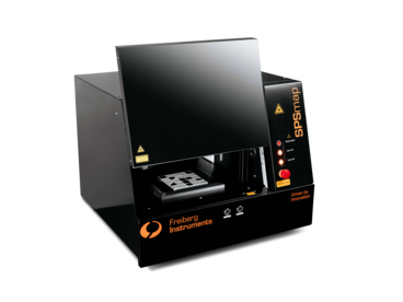
SPS/SPV series
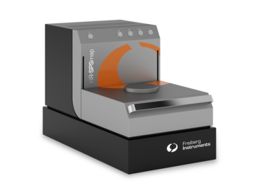
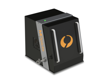
MDP series

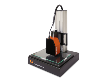
SPS/SPV series
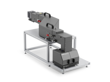
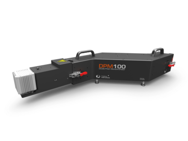
DPM series
Our Partners

