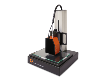
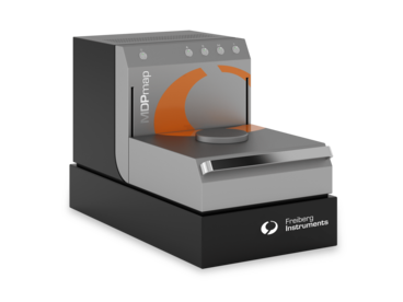
With MDPmap and MDPingot it is possible to measure the resistivity of wafers or bricks with a high accuracy and a resolution of 1 mm via eddy current measurements. The Eddy current sensor setup has a very good long-term stability, due to a distance correlated internal calibration matrix. Hence, with every resistivity map a geometry map of the surface flatness is measured. The resistivity can be measured simultaneously with the minority carrier lifetime and photoconductivity maps. In case of wafer measurements, the thickness of the sample has to be given by the user.
Step width ≥ 1mm
Edge exclusion 12 mm
Resistivity wafer thickness range 150 ...250 µm
Resistivity range can be specified
Default setting: 0.5 to 5 Ohm cm
Accuracy: < 5 %
Repeatability: < 1 % (range of 0.5 until 3 Ohm cm)
It is possible to map the sheet resistance of the emitter, in order to investigate the homogeneity of the emitter diffusion. The resistivity of the base has to be given by the user.
Sheet resistance measurement with range 0.1-200 Ohm/sq
Accuracy at standard sample size,
0.1 - 10 Ohm/sq: < 3 % accuracy
10 - 100 Ohm/sq: < 4 % accuracy
100 – 200 Ohm/sq: < 5 % accuracy
Figure 1 to 3 show examples of resistivity maps measured on mc-Si wafers and bricks.
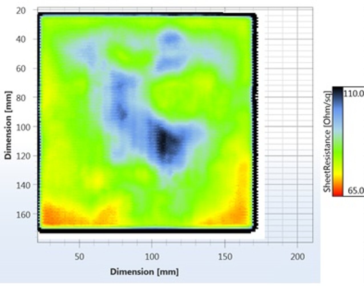
Fig 1: Emitter sheet resistance map of a typical mc-Si wafer with emitter diffusion and an average sheet resistance of 85.1 Ohm/sq.
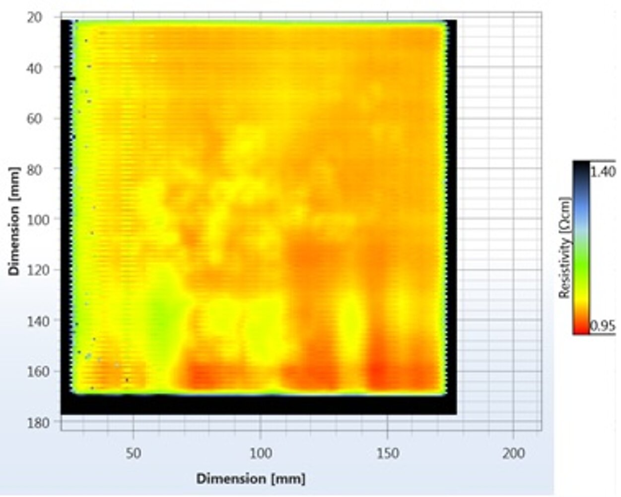
Fig. 2: resistivity map of a typical mc-Si wafer for PV applications and an average resistivity of 1.0 Ohm cm
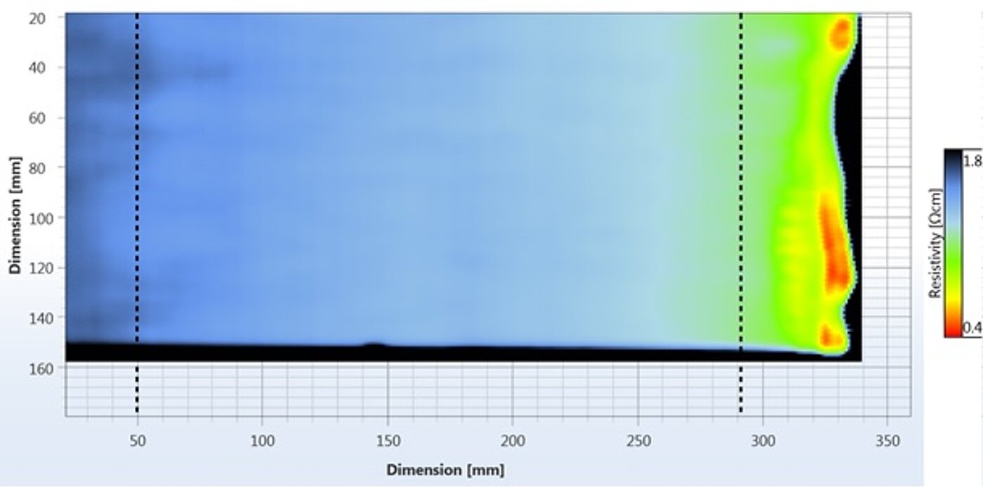
Fig. 3: Resistivity map of a typical mc-Si brick for PV applications and an average resistivity of 1.4 Ohm cm
Related Solutions and Industries: Epitaxial Layers & Thin Films, Photovoltaic