Enables root cause analysis of deep material defects: destruction free, flexible and precise
High temperatures for investigation of deep defect
Customized laser and optic integration for all your materials
Fully automated temperature dependent measurements
Materials
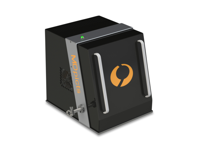
The HTpicts is specialized on deep defects in wide bandgap semiconductors
SiC GaN AIN Ga₂O₃ Diamond and more
Features & Benefits
355–1550 nm
Available wavelengths
10 ns
Time resolution
300–800 K
Temperature range
Extensive
analysis
Large software package