Enables advanced material research for thin layers and surfaces: destruction free, flexible and fast
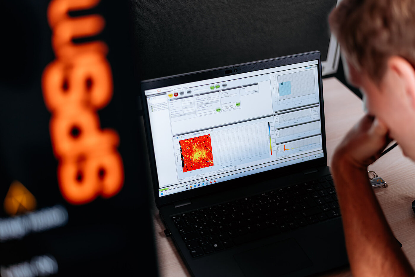
Highly sensitive due to an advanced electronic detection system
Customized lasers and optics for up to 4 different wavelengths
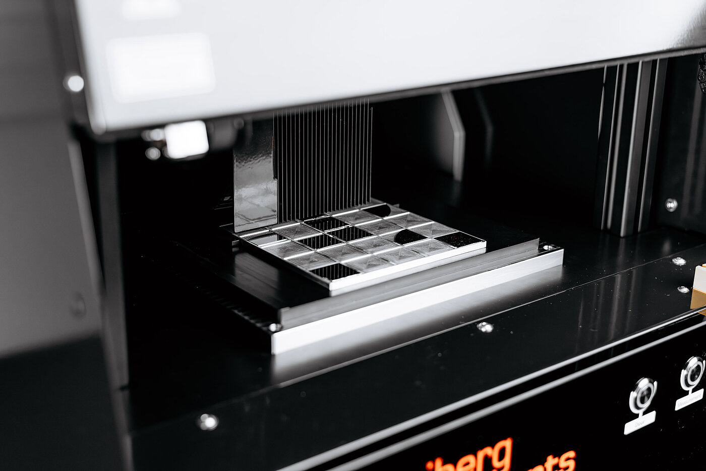
Automatic temperature dependent measurement and/or annealing steps for up to 25 samples
Materials
The SPSmap heat has a versatile range of exciting lasers and enables the electrical characterization of almost all semiconductors
Perovskite Si SiC Ge GaAs InP Ga₂O₃ Diamond
Features & Benefits
355…1550 nm
Available wavelengths

0.1 mm
Spatial resolution
10 ns
Time resolution

Up to
25 samples
Auto. measurement and heating sequence
Applications
Technical specifications
| sample size | wafers or thin slabs up to 25 mm thickness, 5 x 5 mm2 to 160 x 160 mm, square wafers |
|---|---|
| excitation | select up to four different wavelengths from 337 nm up to 1550 nm (default 980 nm) |
| material | Perovskite or any photoactive material (contact us for consultation on your material) |
| measureable | time-resolved and temperature dependent surface photovoltage measurements |
| dimensions | 750 x 835 x 660 mm |
| weight | app. 120 kg |
| power | 100 - 250V, 50/60 Hz, 5 A |
| resolution | 100 µm |