Enables fast and easy assessment of the lifetime at a single point
Single point measurement
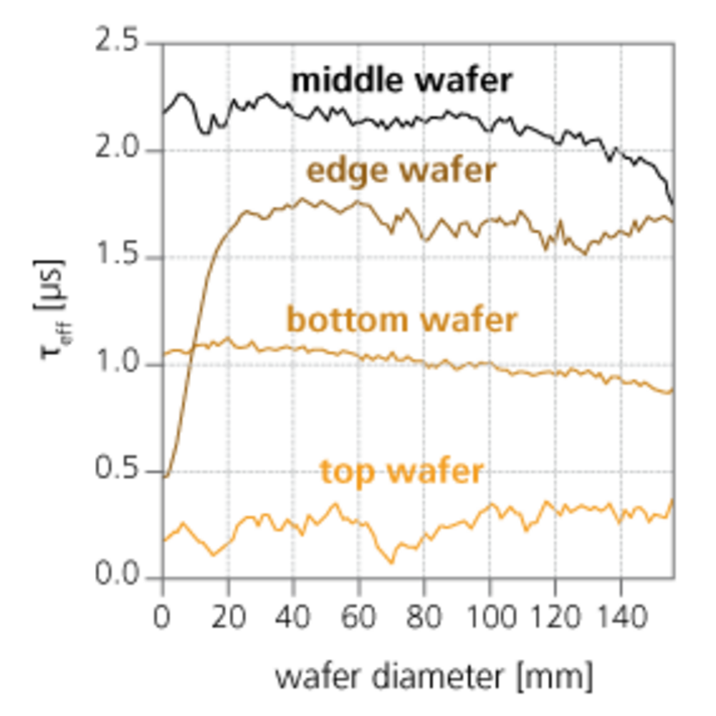
Wafers and ingots
Flexible low cost tool
Materials
Discover unparalleled ease and speed in lifetime characterization of almost all semiconductors with MDPspot, designed to streamline your workflow without compromising accuracy.
Features & Benefits
355–1550 nm
Available wavelengths
10 ns
Time resolution
> 99 %
repeatability
Flexible
measurement
For wafers and ingots
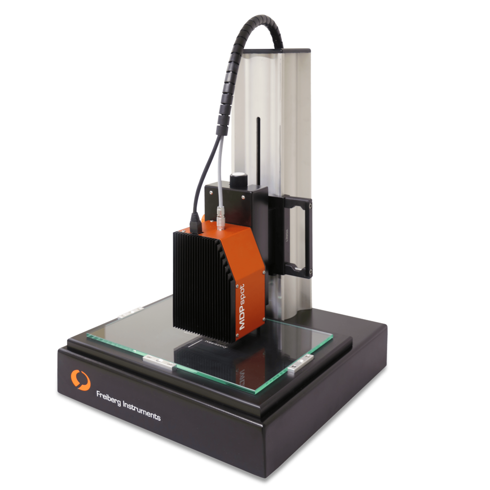
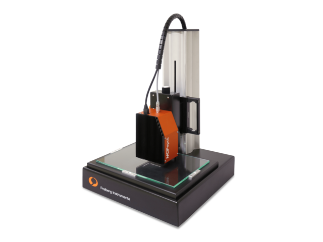
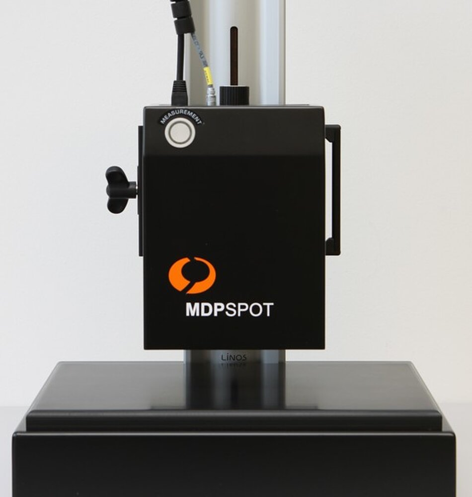
Table top single spot measurements
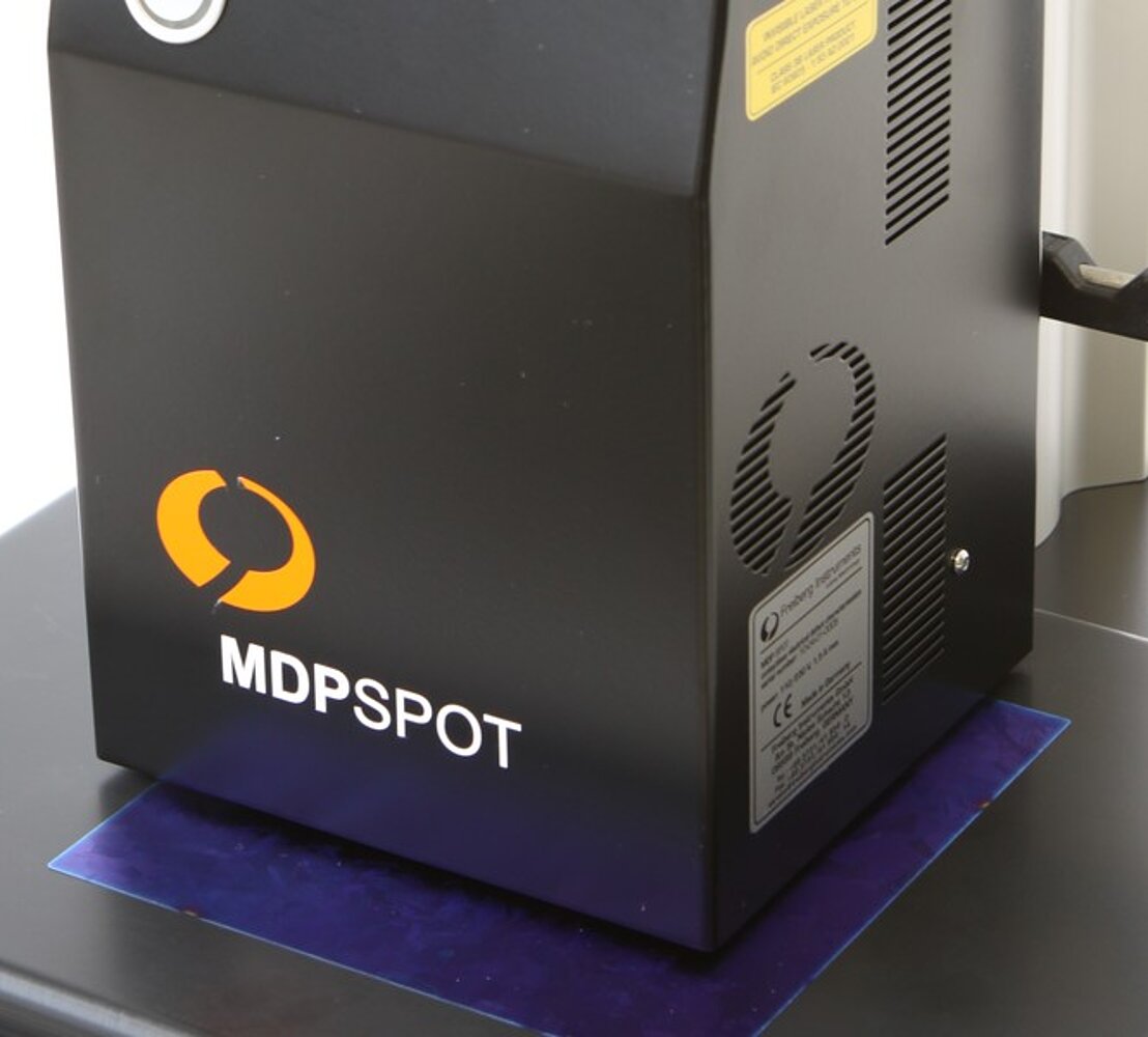
The MDPspot is an affordable and compact solution for lifetime characterization of various semiconductors across different preparation stages. Designed without built-in automation, it offers flexibility for diverse applications.
Cost-Effective Design: A budget-friendly option for reliable lifetime measurements.
Versatile Compatibility: Suitable for a range of semiconductors samples, from thin wafers to thicker materials up to 156 mm bricks.
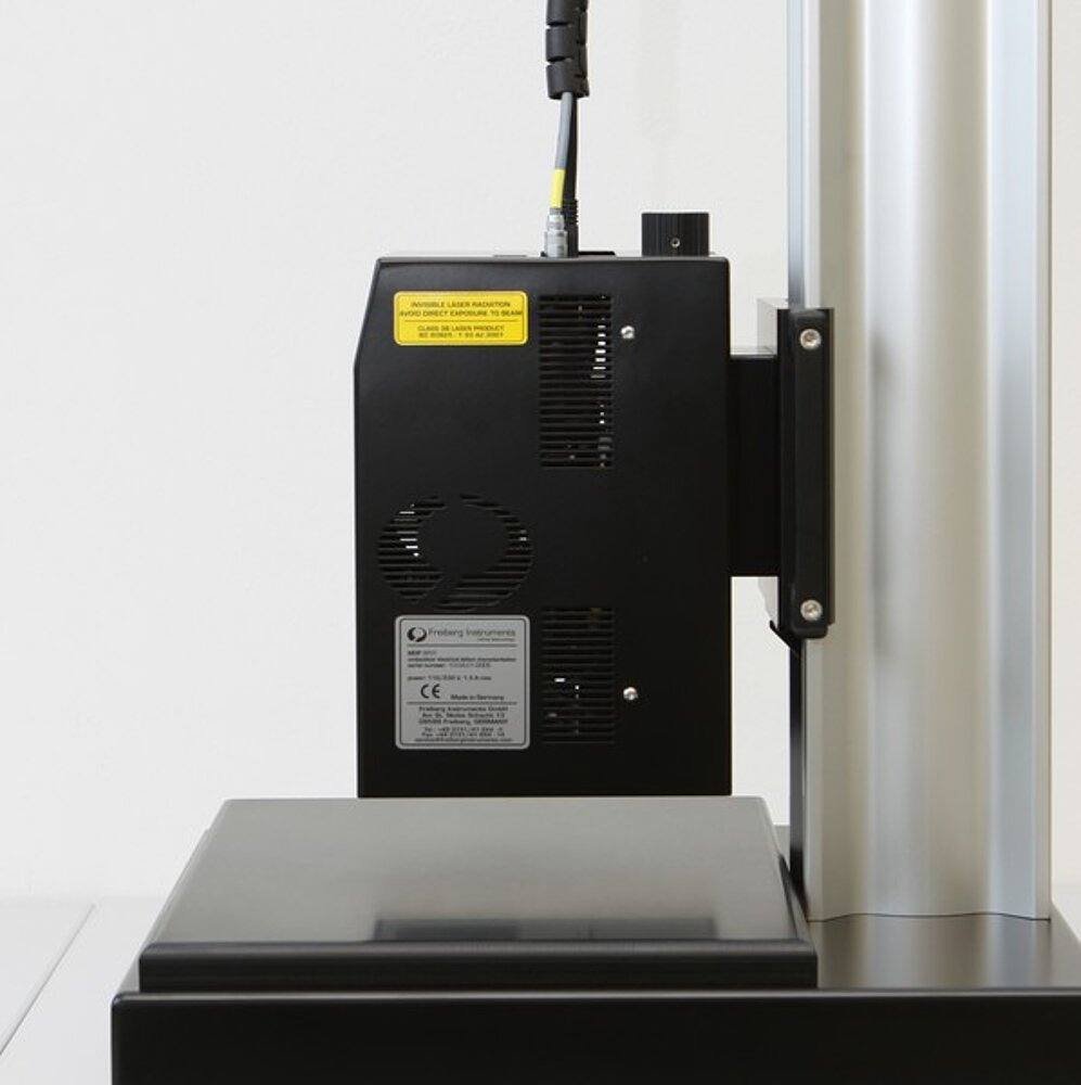
Optional Z-Axis Adjustment: A hand-operated z-axis is available for precise handling of thicker samples.
Intuitive Software: Standard software included for clear visualization and analysis of results.
Streamline your measurement processes with this efficient and easy-to-use system.
Applications
Technical specifications
| mono or multi silicon wafers, bricks, cells, wafers after different processing steps like passivation or diffusion | |
|---|---|
| sample size | above 50 x 50 mm² up to 12“ or 210 x 210 mm² |
| resistivity | 0.2 - 10³ Ohm cm |
| material | silicon wafers, bricks, partially or fully processed wafers, compound semiconductors and beyond |
| measureable properties | carrier lifetime |
| dimension | 360 x 360 x 520 mm, weight: 16 kg |
| power | 110/220 V, 50/60 Hz, 3 A |