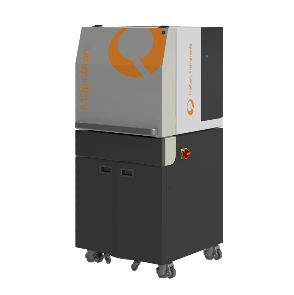
Enables root cause analysis of material defects: destruction free, flexible and precise
High spatial resolution
Customized laser and optic integration for all your materials
Novel cryostat for samples up to 4’’
Materials
The MDpicts pro enables the electrical characterization of almost all semiconductors
Si SiC Ge GaAs Ga₂O₃ InP Diamond and more
Features & Benefits
355–4600 nm
Available wavelengths
10 ns
Time resolution
83–300 K
Temperature range
10 µm
Spatial resolution
Applications
Technical specifications
| temperature range | 83 – 350 K |
|---|---|
| sample size | up to 4" wafers small wafer pieces |
| resistivity | 0.2 - >1010 Ωcm |
| conduction type | p,n |
| minority carrier lifetime | 20 ns – 100 ms |
| measurable properties | lifetime, photoconductivity, activation energy, etc. |
| excitation | 355 – 4600 nm |