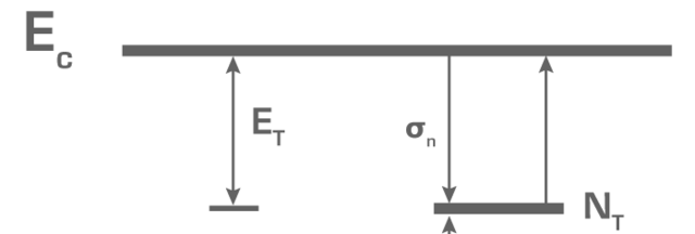
Electrical Characterization
The performance of semiconductor devices depends fundamentally on key electrical parameters of the material and therefore also on defect densities and their electrical properties.
Even in a single crystal, the crystal orientation can exhibit small changes over the surface, which result from internal strains caused by lattice defects. Orderly grown thin films can also have an interesting in-plane orientation distribution.
Mapping a surface requires a lot of measurements. Here the Omega Scan method can offer its advantage in speed. The picture shows an orientation map measured on a (Si, Ge) solid solution wafer . The maximum orientation difference is 0.03°. Concentric circles follow the growth rings of the crystal.

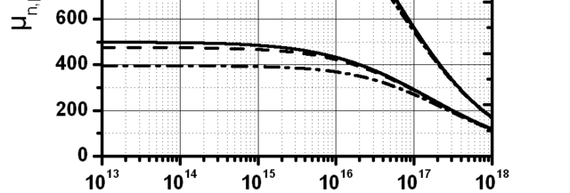

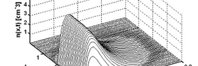
Simulation of carrier profiles
For a better understanding of lifetime measurements and to achieve a better comparability between different measuring methods, it is necessary to perform simulations.