Materials
For HJT, HIT, TOPcon, bifacial PERC, PERC+ solar cells and more.
Si Perovskite and more
Features & Benefits
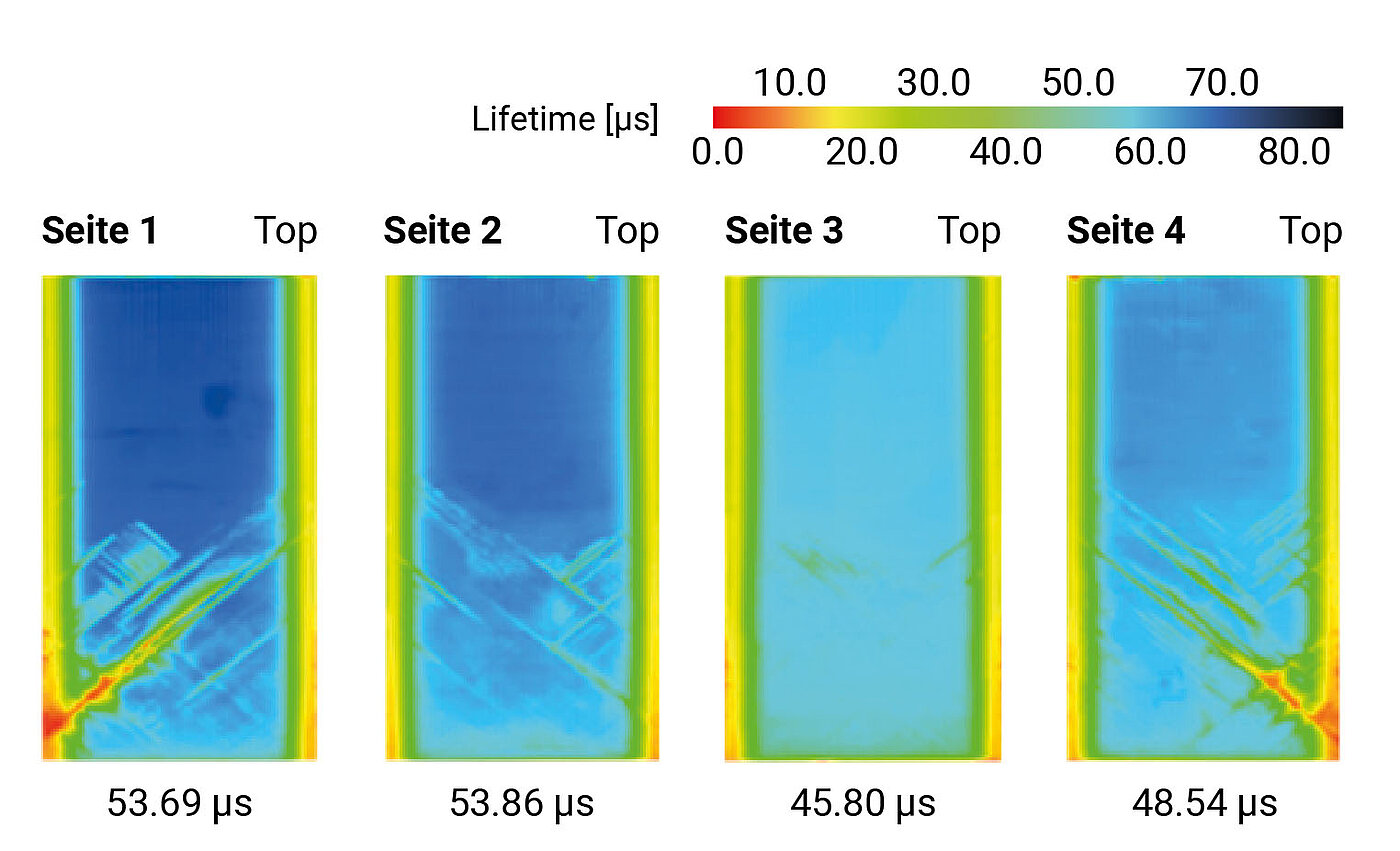
Slip lines in Cz-Si ingot
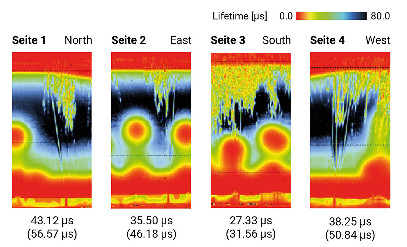
Lifetime measurement of a quasi-mono Si ingot with a lot defects
Applications
Technical specifications
| Material | monocrystalline silicon |
|---|---|
| Ingot size | between 125 x 125 to 210 x 210 mm², brick length 850 mm or longer |
| Wafer Size | up to 300 ¬mm diameter |
| Resistivity range | 0.5 – 5 Ohm cm. Other ranges on request |
| Conduction type | p, n |
| Measurable properties | lifetime - μPCD/MDP (QSS), photoconductivity, resistivity and more |
| Default excitation | lR laser diode (980 nm, max. 500 mW) and IR laser diode (905 nm, max. 9000 mW). Other wavelengths are available on request |
| PC workstation | Windows 11 or latest, .NET Framework update, 2 Ethernet ports |
| Power requirements | 100 – 250 V AC, 6 A |
| Dimensions (W × H × D) | 2560 × 1910 × 1440 mm |
| Weight | approx. 200 kg |
| Certification | manufactured under ISO 9001 guidelines, CE conform |


