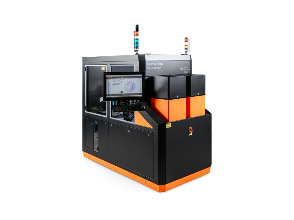
Use precise wafer orientation data where it creates the most value.
Fast and precise measurement: Hybrid X-ray and optical metrology delivers reliable orientation data within production workflows.
Designed for fab automation: SMIF loadports, OHT-ready handling and flexible communication options enable seamless integration.
Ready for changing requirements: Process wafer sizes from 70 to 300 mm and a wide range of crystalline materials.
Materials
One platform for multiple wafer materials. Measure a wide range of crystalline wafer materials with one flexible metrology platform.
Features & Benefits
70–300 mm
Scalable wafer size range
0.003˚
Offcut magnitude precision
Flexible
Loading and communication options
Hybrid
X-ray and optical metrology (Omega Scan)
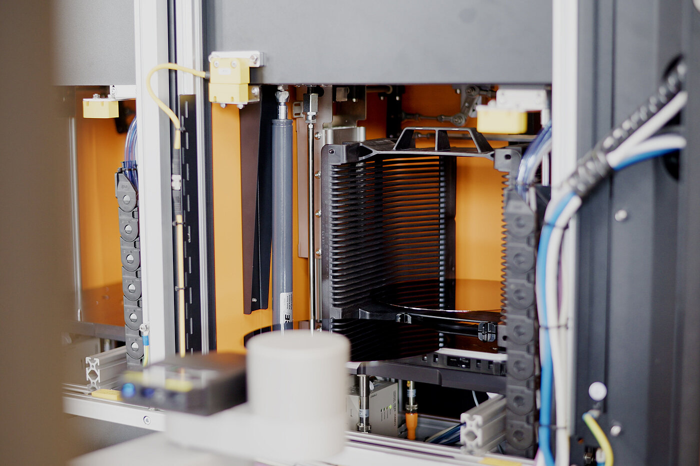
Wafer carrier for automated high-through put handling
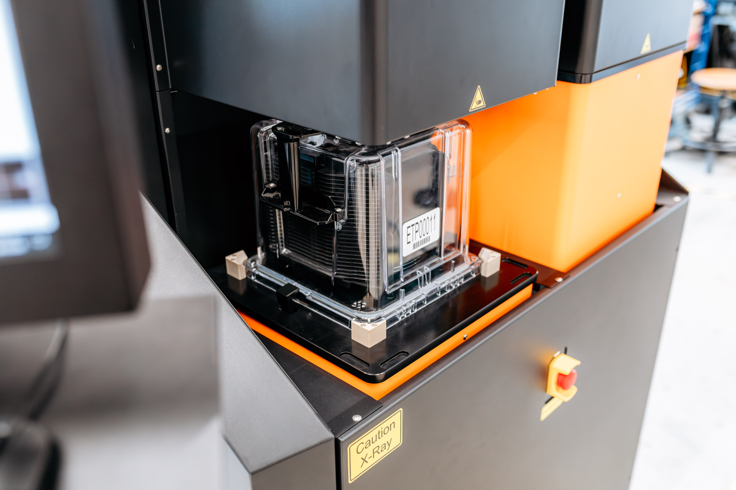
External robot loading ports for fab automation
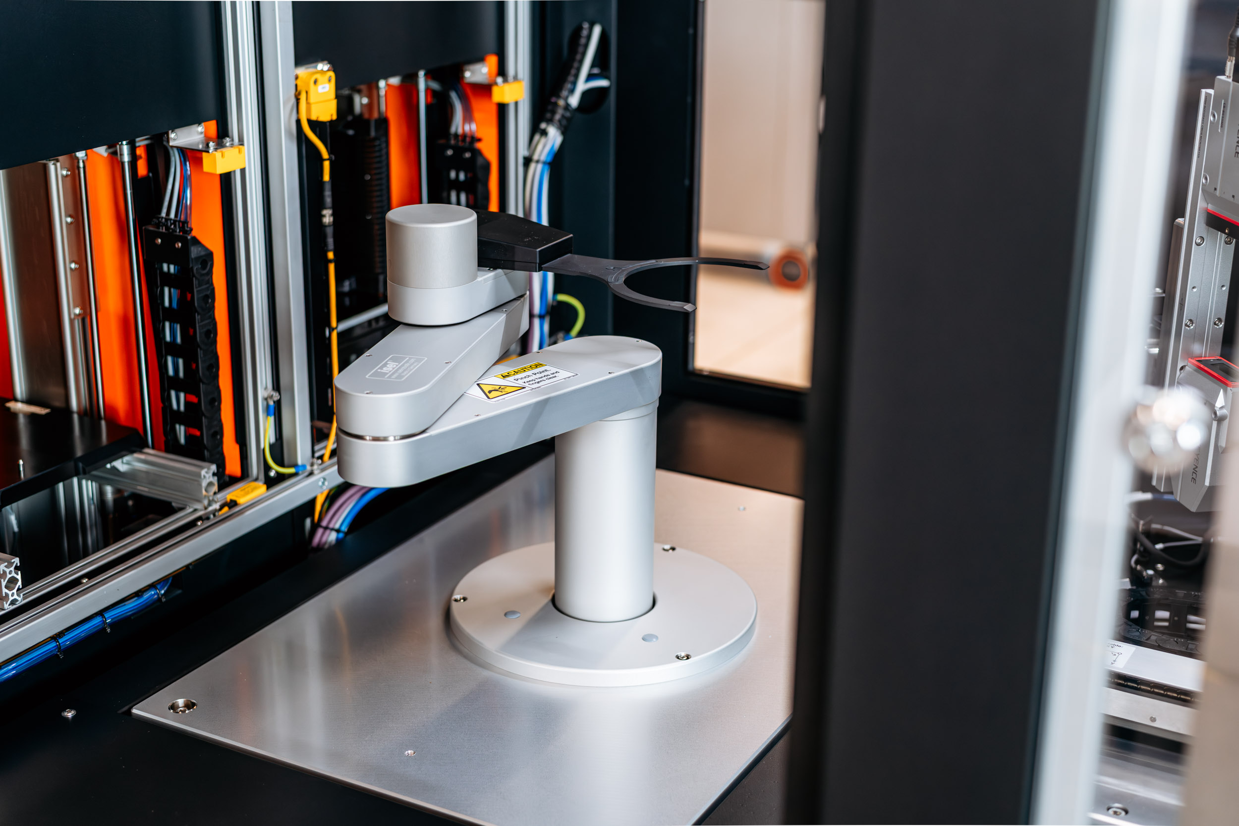
Wafer handling robot
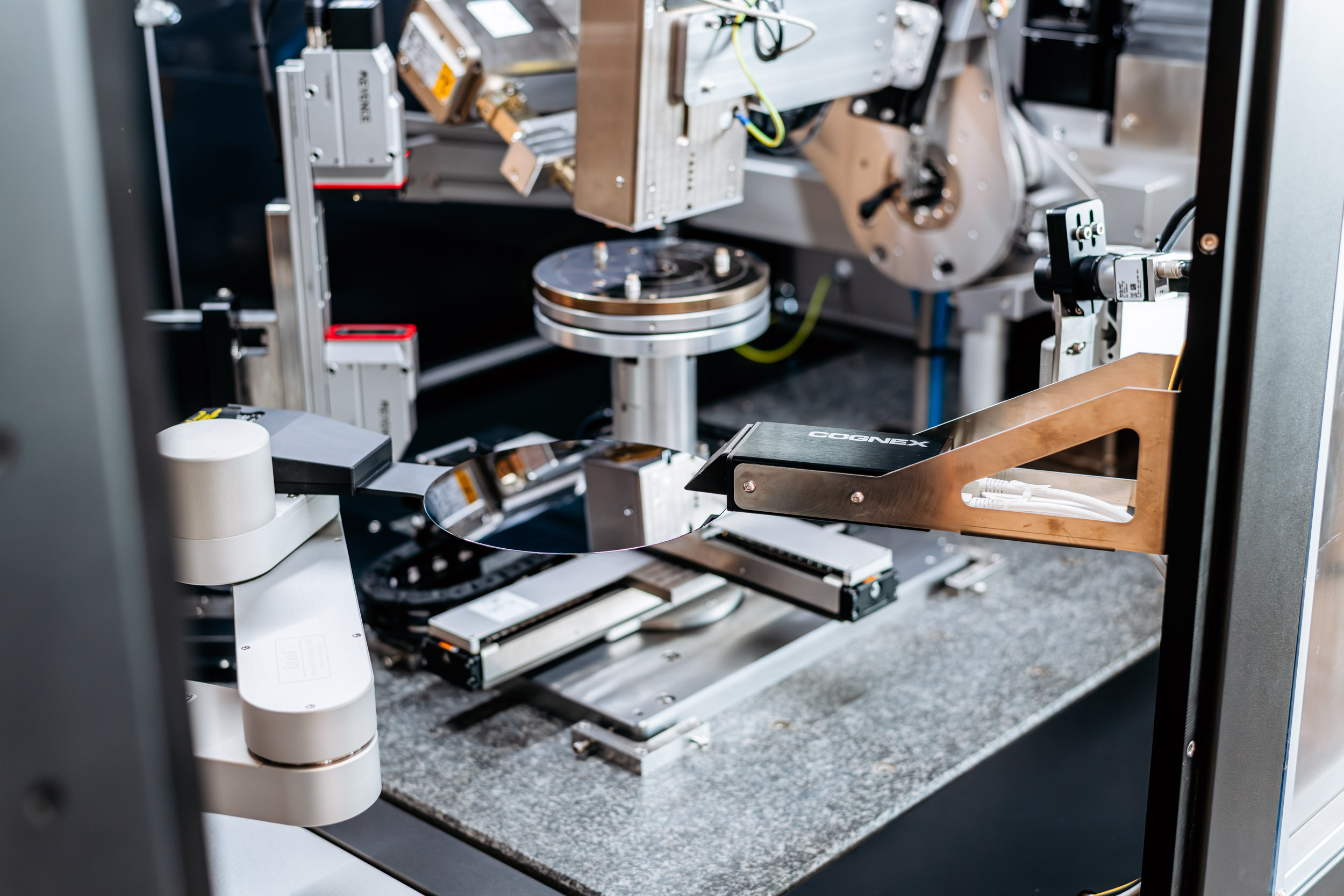
Wafer tracking with ID reader
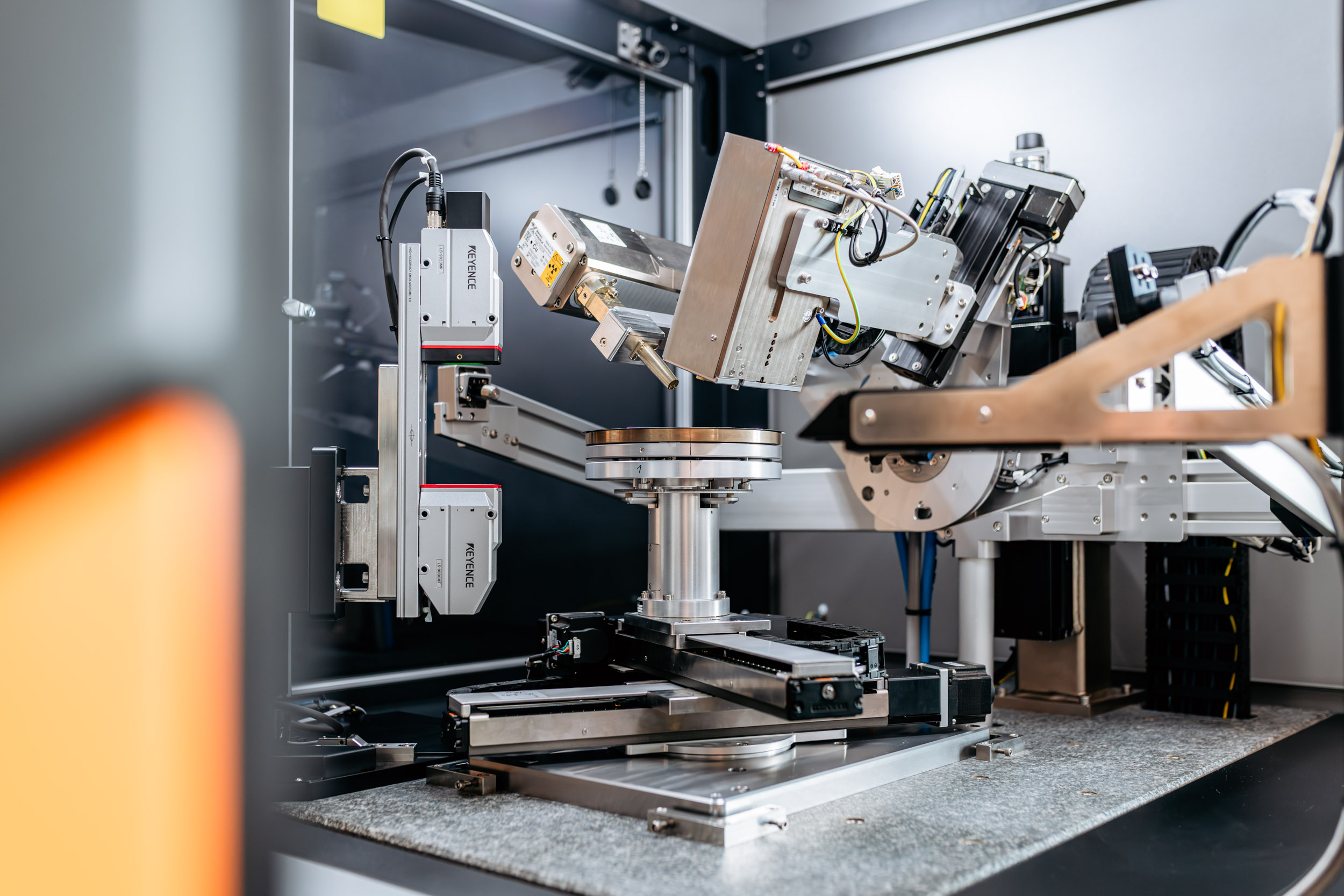
XRD and geometry measurement setup

High-precision wafer mapping stage
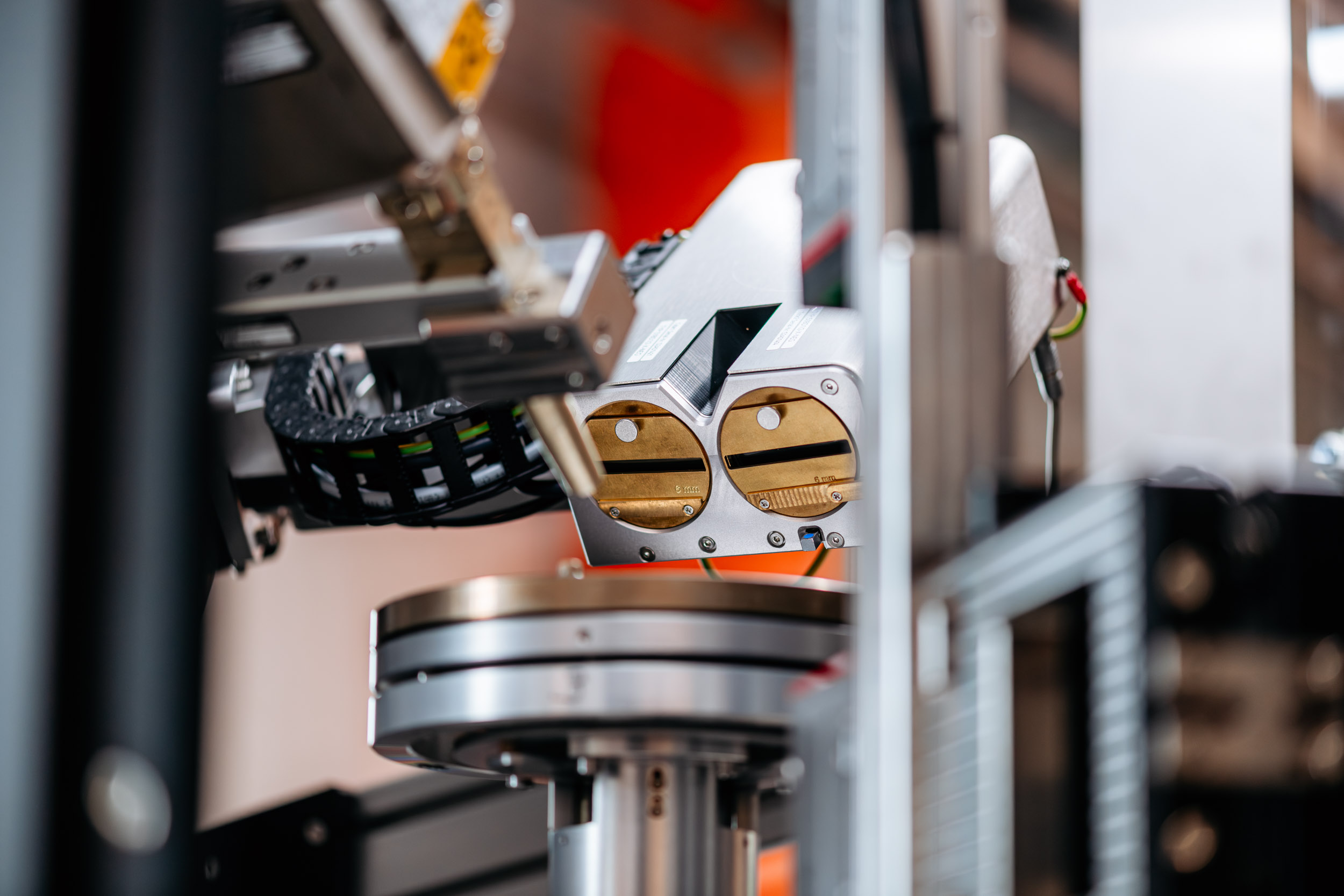
X-ray double detector
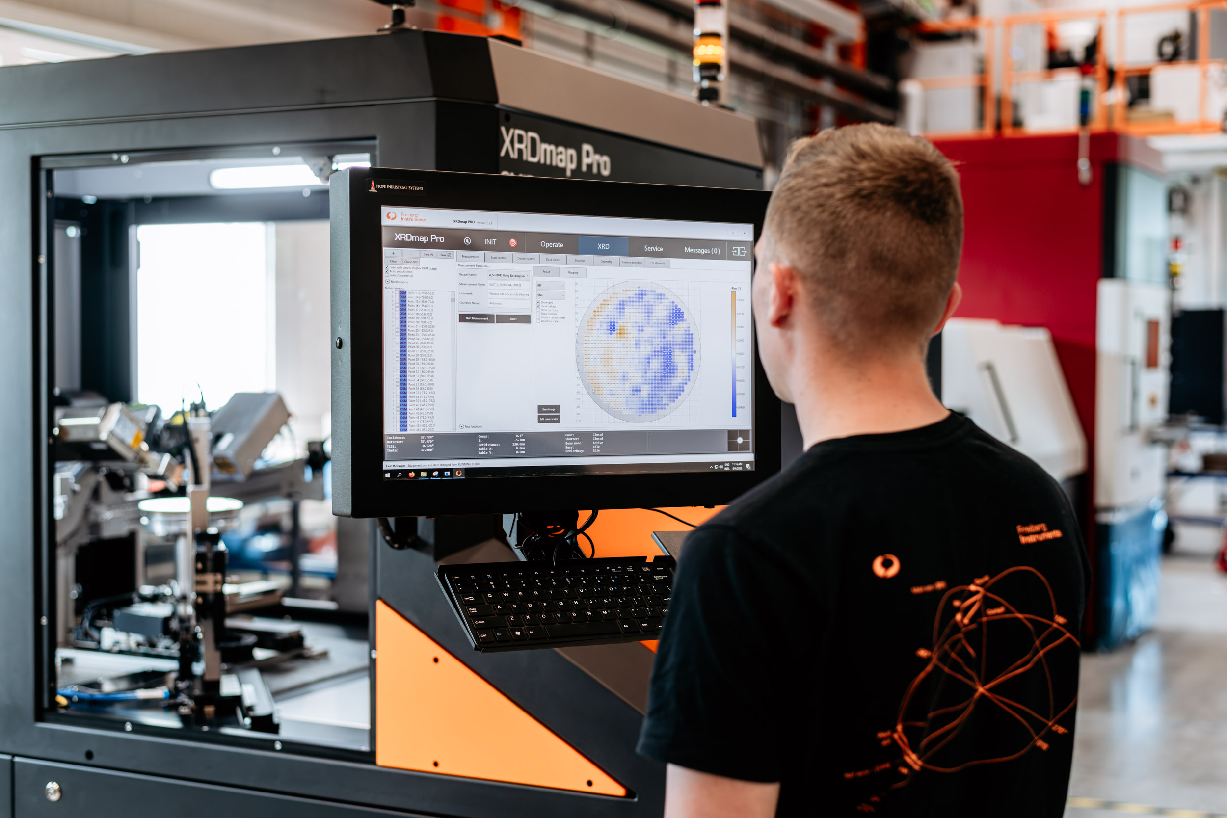
Data acquisition and evaluation interface
Applications

With an offcut magnitude precision better than 0.003°, XRDmap Pro delivers benchmark-leading measurement results to optimize downstream processes such as epitaxy, lithography and ion implantation.
Dr. Christian Hagendorf
Key Account Manager
Specifications
| Precision | 0.003°/<0.03° (1σ) on off-cut (tilt) and in-plane (twist) |
|---|---|
| XRD | Omega scan X-ray crystal orientation (5s/measurement) |
| Geometry | Notch (optical sensor) |
| Materials |
|
| Samples | 70 – 300 mm wafer |
| Measurements |
|
| Automation | Robot handling (60 wafers/hour), 2 SMIF ports |
| Fab communication | SECS/GEM |
| Processes | Epitaxy, lithography, ion implantation |
| Dimension (w × h × d) | 2250 × 1250 × 2476 mm |