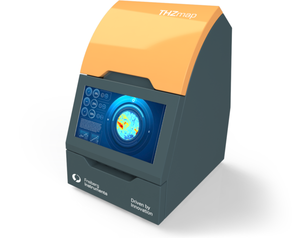
High-precision mapping system based on THz time-domain spectroscopy designed for epitaxial layers on highly doped materials
Non-Destructive & Non-Contact
Optimized for thin layers on Highly Doped substrates
High spatial resolution of 1mm
Materials
THzmap is specialized on highly doped materials.
Features & Benefits
Sigma < 1 %
Very good repeatability
± 5 %
Accuracy depending on thickness
Throughput
> 5 Wafers
per hour
3 mm
Edge exclusion
In semiconductor manufacturing, the difference between peak performance and failure lies in the micrometer range. Our latest Mapping System, powered by Terahertz Time-Domain Spectroscopy (THz-TDS), delivers a breakthrough in characterization – specifically engineered for epitaxial layers on challenging, highly doped substrates.
Breaking the Conductivity Limit
Traditional optical and eddy current methods often struggle with the high absorption and conductivity of heavily doped substrates. Our THz-TDS technology utilizes reflection-mode measurement to bypass these limitations, allowing for ultra-precise analysis of epi-layers where transmission-based systems fail.
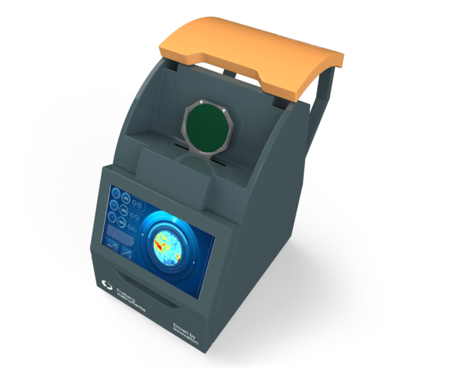
Measure with zero risk of surface contamination or mechanical damage to your wafers. Visualize electrical homogeneity across the entire wafer with spatial resolutions down to 1 mm, identifying process drifts before they impact yield. Replace slow, destructive methods like Mercury-CV or SIMS with a rapid, inline-capable THz solution.
Our THz-TDS Mapping System provides the critical data needed to optimize reactor performance, minimize scrap, and ensure the reliability of power electronics and RF components.
In semiconductor manufacturing, the difference between peak performance and failure lies in the micrometer range. Our latest Mapping System, powered by Terahertz Time-Domain Spectroscopy (THz-TDS), delivers a breakthrough in characterization – specifically engineered for epitaxial layers on challenging, highly doped substrates.
For bulk samples: 0.1 to 100 ohm cm
For epitaxial layers: 8 × 1015 cm-3 to 4 × 1018 cm-3
Applications

THzmap enables to measure the unmeasurable – accurate epi resistance on highly doped substrates.
Dr. Nadine Schüler
Head of Research & Development
Specifications
| Measured parameter | Resistivity / doping density |
|---|---|
| Measurement principle | Contactless and non-destructive Terahertz Time-Domain Spectroscopy (THz-TDS) |
| Result | Full wafer maps |
| Resolution | 1 mm |
| Measurement time | 20 min for 12’’ wafer |
| Power supply | 100 – 250 V (± 10), 5A, single phase |
| Dimension (w × h × d) | 670 × 490 × 810 mm |
| Minimum sample size | 10 × 10 mm |
| Maximum sample size | Wafers up to 150 mm diameter (larger on request) |
| Sample thickness |
|

Accessories & Options
Automation of sample handling possible