Figure 1 shows an example using SPV for the characterization of the polishing process on the double-side polished high-resistivity float zone silicon wafer. The red areas in the plots clearly show that the CMP polishing process is not optimal and even signatures of a handling tool are clearly visible in the plots (left below).
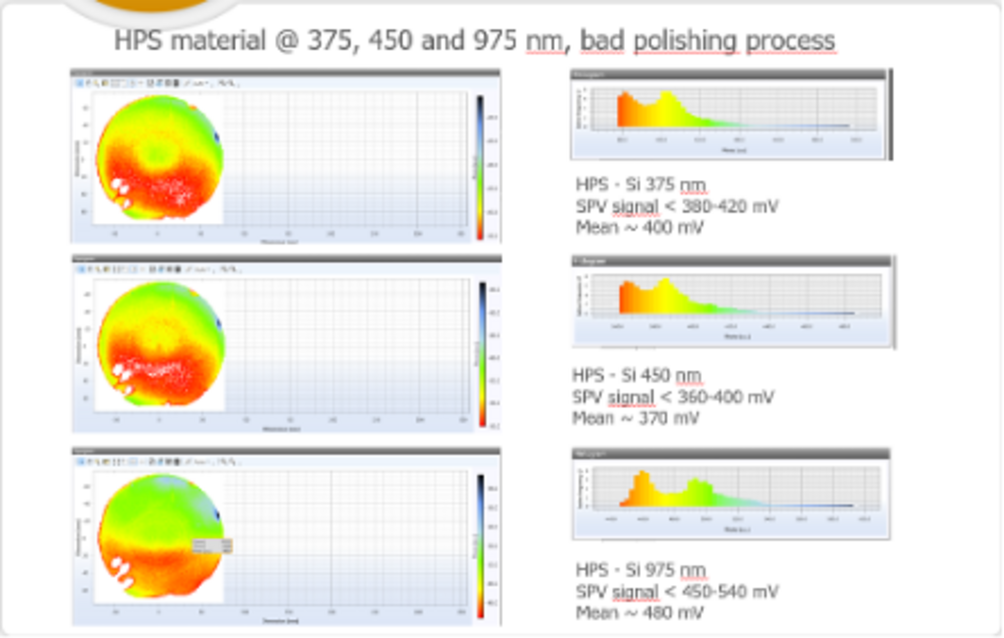
Fig. 1: Using SPV for the characterization of the polishing process