Choose another division
Electrical semiconductor characterization
Luminescence dating, research, dosimetry and more
Contamination monitor, beta-aerosol monitor, dose rate meter and more
for ultra-fast crystal orientation, crystal alignment in production, quality control, rocking curve measurements, material...
state-of-the-art XRD system for automatic single crystal ingot orientation, tilting and alignment for grinding
Wafer sorting, crystal orientation, resistivity, optical notch and flat determination
Flexible diffractometer for ultra-fast Omega Scan orientation determination
Smart diffractometer for ultra-fast Omega-scan of small samples.
Robust XRD equipment for fully automated in-line testing & alignment
for blanks, wafers & bars (AT, SC, TF, etc.)
three generations of X-ray engineers
in industrial production, R&D and more
discover the most convenient way of measuring orientation of single crystals
Mono- and Multi-crystalline wafer lifetime measurement device
Low cost table top lifetime measurement system for characterization of a variety of different silicon samples at different...
Mono- and Multi-crystalline wafer and brick lifetime measurement device
for production and quality control of monocrystalline Si ingots,bricks and wafers
Flexible OEM unit for lifetime measurements at a variety of different samples ranging from mono- to multicrystalline silicon...
for contactless and temperature dependent lifetime and LBIC measurements
High Resolution Resistivity Mapping Tool for process control and quality assurance measurements
The minority carrier life time is sensitive for all kinds of electrically active defects in semiconductors and is therefore...
MDP is an advanced technology with a so far unsurpassed combination of sensitivity, speed and resolution for fab and lab...
High sensitivity, high resolution surface photovoltage (SPV) measurement instrument
High sensitivity, high resolution surface photovoltage spectroscopy (SPS) instrument with a variable energy excitation source...
for quality control of bifacial PERC/PERC+ solar cells and more
portable in field PID tester for solar modules
user friendly and advanced operating software
The PIDcon devices are designed to investigate the PID susceptibility for production monitoring of solar cells as well as tests...
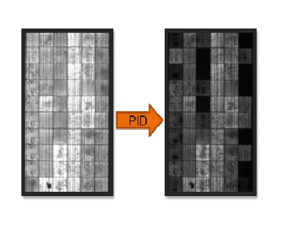
Learn more about the reasons for PID and the how the susceptibility of solar cells, mini modules and encapsulation materials can...
Our quality management system is an integrated process-oriented system with ISO 9001 certification.
In order to establish a criterion for the pass or fail of the PID test the conductance test and the power loss are used.
In order to establish an easy way to decide whether a solar cell or mini-module has a PID problem or not, even though the operator itself has not the physical background the power loss is determined and given as an output by the software PIDStudio. It shows the expected relative power loss of the degraded area of the cell under STC (1000 W/m2) following the formula:
∆P: Absolute power lossP0: Nominal power under standard test conditions (STC) = 1000 W/m2 irradiance∆P/P0: Relative power loss under STC conditions (approximate value, valid for power loss up to ~30%)Vmpp: Voltage at maximum power (= 0.5 V for standard silicon solar cells)Impp: Current at maximum power (= 8 A for standard silicon solar cells at STC)Rp: Measured parallel resistance (= V/I as measured between front and back contact for the whole cell)Acell: Cell area (= 243 cm² for standard silicon solar cells)Apid: PID-tested area (= 100 cm² for standard PIDcon setup)
Furthermore an easy pass or fail criterion after finishing the PID measurement is suggested. It is assumed that an efficiency loss of 3% at the end of the PID test lead to a fail of the solar cell (according to IEC-Standard). The measurement time therefore is 168 h at room temperature or 72 h at 85 °C (recipe “Long”). An efficiency loss of 3% is equal to an increase of the cell’s conductance of 150 mS for the tested area, meaning 1.5mS/cm2 related to the 100 cm2 electrode size. The formula for calculating the conductance is as follows:
So it is the reciprocal of the parallel resistance related to the degraded area. If the PID diagram of a cell after 72 h shows a higher conductance increase as 1.5 mS/cm2, it fails the test and has a PID problem and should be sorted out, otherwise it will pass it. Please keep in mind that the test is not for absolute value of conductance, but only for increase of conductance (Conductance at the start point is unequal to zero).
Please notice that the curves “Power loss” and “Conductance” look equal in the auto focus option, since the formulas are comparable.
To save measurement time, the recommended measurement time is shortened to 4 hours. The fail criterion for that time span is 0.1 mS/cm2 at 1000 V and 85 °C. Keep in mind that this criterion is only a hint for a PID problem, a conductance increase of 0.1 mS/cm2 in 4 h will not lead to a measurable power loss. Therefore it is in the customer’s responsibility to check and use this fail criterion. Same applies for the recipe “Fast” with a fail criterion of 0.025 mS/cm2 after 1 h. Nevertheless usage of higher measurement times (minimum 4 hours) is strongly recommended.
µPCD/MDP (QSS)
PID
X-ray diffraction
Projects
Company
This Website uses cookies Our website uses cookies and the web analytics tool Google Analytics according to our privacy policy. By continuing to browse these pages, you agree. If you do not want to collect data from Google Analytics, you can disable this here