Enables advanced material research for thin layers and surfaces: destruction free, flexible and fast
Highly sensitive due to an advanced electronic detection system
Customized lasers and optics for up to 4 different wavelengths
Investigation of charge separation processes and electronic transitions (defects)
Materials
Features & Benefits
355–1550 nm
Available wavelengths
10 ns
Time resolution
0.1 mm
Spatial resolution
< 5 min
Throughput for 8’’ wafer
Flexible Mapping Tool for R&D and Production Monitoring
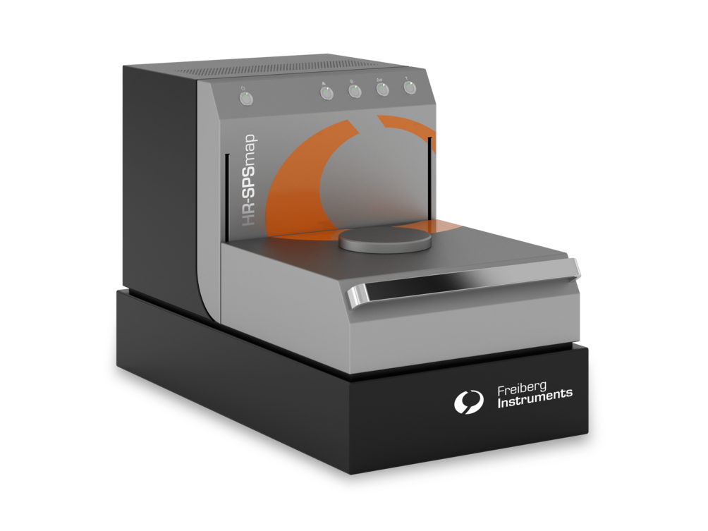
The HR-SPSmap product platform builds on the proven foundation of the widely acclaimed MDPmap series. This compact, benchtop, contactless electrical characterization tool is specifically designed for offline production control and research and development applications. It measures surface photovoltage (SPV) across a wide injection range, accommodating both steady-state and short-pulse excitation. With automated sample recognition and parameter setup, it effortlessly adapts to a diverse range of samples, including epitaxial layers and wafers at various stages of processing, from as-grown material to fully fabricated devices.
Exceptional Flexibility and Advanced Features
One of the standout advantages of the HR-SPSmap is its exceptional flexibility. Equipped with fixed-energy excitation sources, the system supports the integration of up to four lasers within the measurement head. This capability facilitates injection-level-dependent SPV measurements across a broad range, from very low to high injection levels, and enables depth profiling using different laser wavelengths. The system also includes a bias light feature for enhanced measurement options.
In addition, the HR-SPSmap supports custom calculations and mapping configurations, along with the ability to export primary data for detailed external analysis. For standard metrology tasks, the platform offers a predefined recipe system, allowing routine measurements to be completed with a single button press.
Unlock Precision and Adaptability
With its advanced capabilities and user-friendly design, the HR-SPS is the ideal solution for researchers and production teams seeking high-precision surface photovoltage measurements. Whether for R&D innovation or reliable production monitoring, this platform redefines flexibility and efficiency in electrical characterization.