Aim
Ga2O3 is an ultra-wide band gap semiconductor with a great application potential. The contactless characterization of defect related transitions with high sensitivity is still challenging.
Solution
Contactless surface photovoltage (SPV) spectroscopy in the dc (Kelvin probe, direct measurement of the contact potential difference, DCPD) and ac (modulated regime) modes provides information about transitions energies and direction of charge separation in a wide spectral range from near infrared (< 0.5 eV) up to the deep ultraviolet (> 6 eV) at high sensitivity. Furthermore, the same perforated electrode can be applied for measurements in dc and ac modes with a charge amplifier (figure 1).
Application example
Figure 2 shows an example for the measurement of a (negative) DCPD spectrum and the spectrum of the modulated SPV amplitude (in a logarithmic scale) on the same place of a b-Ga2O3 crystal. Transitions at the band gap of b-Ga2O3 at 4.8 eV and defect transitions at 1.6, 2.3, 3.2, 4.0, 4.4 and 4.6 eV are well distinguished whereas the sensitivities for measurements in the dc and ac modes can be rather different for different transitions.
References
[1] Th. Dittrich, S. Fengler, N. Nickel, “Surface photovoltage spectroscopy over wide time domains for semiconductors with ultrawide bandgap: example of gallium oxide”, Phys. Stat. Sol. A 11 (2021) 2100176.
![Fig. 1: Scheme for the measurement in dc and ac modes with the same electrode and a charge amplifier [1].](/fileadmin/_processed_/6/b/csm_characterization_of_ga2O3_01_b03995671e.png)
Fig. 1: Scheme for the measurement in dc and ac modes with the same electrode and a charge amplifier [1].
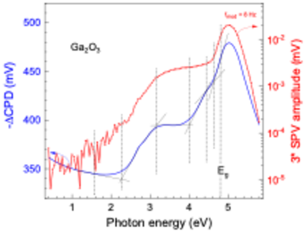
Fig. 2: Spectra of DCPD (blue) and spectrum of the modulated SPV amplitude (red) of a b-Ga2O3 crystal. Onsets at major defect transitions and at the band gap.
Related Solutions and Industries: Epitaxial Layers & Thin Films