Aim
SiC, GaN and AlGaN belong to the class of wide band gap semiconductors and are applied especially in power electronics, optoelectronic devices and transistors such as HEMTs (high electron mobility transistor. The contactless optoelectronic characterization of wide band gap semiconductors and heterostructures under production conditions and in fields of R&D is often challenging.
Solution
SPV spectroscopy in the dc (Kelvin probe, measurement of the contact potential difference, DCPD) and ac (modulated) modes provides information about preferential directed charge separation in relation to electronic transitions and carrier dynamics [1]. The application of charge amplifiers allows for SPV measurements in dc and ac modes with the same electrode.
Application example
Figure 1 shows DCPD spectra of GaN, Al0.25Ga0.75N/GaN and 4h-SiC/GaN deposited onto sapphire wafers. Aside directions of charge separation and transition energies at band gaps, defect transitions can be distinguished. Signatures of slow processes can be discriminated in modulated SPV measurements (figure 2).
References
[1] Th. Dittrich, S. Fengler, “Surface photovoltage analysis of photoactive materials”, World Scientific, 2020.
[2] Th. Dittrich, S. Fengler, N. Nickel, “Surface photovoltage spectroscopy over wide time domains for semiconductors with ultrawide bandgap: example of gallium oxide”, Phys. Stat. Sol. A 11 (2021) 2100176.
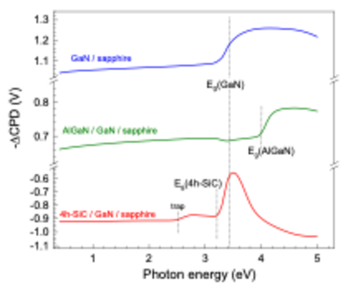
Fig. 1: DCPD spectra of GaN (blue), Al0.26Ga0.74N / GaN (green) and 4h-SiC / GaN (red) epitaxial layers deposited on sapphire.
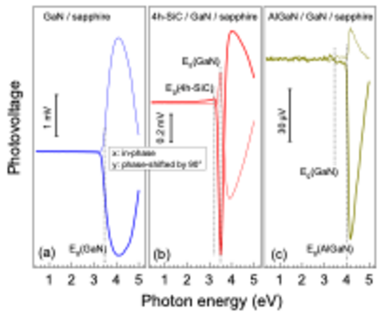
Fig. 2: Modulated in-phase and phase-shifted by 90° SPV spectra of GaN (a), 4h-SiC / GaN (b) and Al0.26Ga0.74N / GaN (c).
Related Solutions and Industries: Epitaxial Layers & Thin Films