Aim
For further development of optoelectronic devices and other applications based on diamond and nanodiamond, contactless characterization of electronic defect states and electronic transitions in bulk diamond and at diamond surfaces over a wide spectral range is of great interest.
Solution
Contactless surface photovoltage (SPV) spectroscopy in the Kelvin probe (direct measurement of the contact potential difference, DCPD) and modulated regimes provides information about transitions energies and direction of charge separation in a spectral range from near infrared (< 0.5 eV) up to the deep ultraviolet (> 6 eV) at high sensitivity.
Application example
Diamond has an ultra-wide indirect band gap of 5.47 eV [1]. Figure 1 shows the DCPD spectrum and its derivative for a polycrystalline diamond sample prepared by CVD. Transitions related to excitation via defect states and transitions around the band gap can be clearly distinguished [2]. For the modulated SPV spectra of another diamond sample, the sensitivity is increased and transitions at 5.258 and 5.544 eV related to absorption assisted by the indirect exciton and transversal optical phonon are well pronounced. Related spectra are like fingerprints and can be used, for example, for inline control in production lines.
References
[1] C. D. Clark, P. J. Dean, P. V. Harris, “Intrinsic edge absorption in diamond”, Proc. R. Soc. London A 277, 312 (1964).
[2] Th. Dittrich and S. Fengler, “Transitions in polycrystalline diamond probed by surface photovoltage spectroscopy”, to be submitted.
![Figure 1: Spectra of DCPD and its deriva-tive for polycrystalline CVD diamond (data after [2]). Onsets at major defect transitions and around the band gap.](/fileadmin/_processed_/b/c/csm_Electronic_transitions_diamond_1_fa9d98c290.png)
Figure 1: Spectra of DCPD and its deriva-tive for polycrystalline CVD diamond (data after [2]). Onsets at major defect transitions and around the band gap.
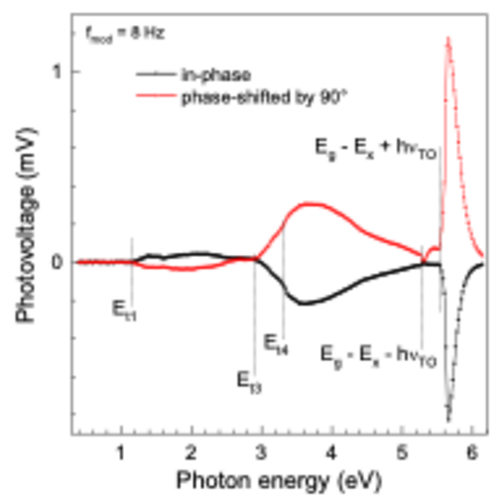
Fig. 2: In-phase and phase-shifted by 90° modulated SPV spectra of a diamond crystal. Dotted lines give defect related transitions and transitions Eg - Ex ± hvTO.
Related Solutions and Industries: Epitaxial Layers & Thin Films