Choose another division
Electrical semiconductor characterization
Luminescence dating, research, dosimetry and more
Contamination monitor, beta-aerosol monitor, dose rate meter and more
for ultra-fast crystal orientation, crystal alignment in production, quality control, rocking curve measurements, material...
state-of-the-art XRD system for automatic single crystal ingot orientation, tilting and alignment for grinding
Wafer sorting, crystal orientation, resistivity, optical notch and flat determination
Flexible diffractometer for ultra-fast Omega Scan orientation determination
Smart diffractometer for ultra-fast Omega-scan of small samples.
Robust XRD equipment for fully automated in-line testing & alignment
for blanks, wafers & bars (AT, SC, TF, etc.)
three generations of X-ray engineers
in industrial production, R&D and more
discover the most convenient way of measuring orientation of single crystals
Mono- and Multi-crystalline wafer lifetime measurement device
State of the art system for topographic electrical characterization of multicrystalline bricks in fabs with high throughput....
Production integrated high speed wafer mapping of carrier lifetime. Single wafer topograms in less than one second a wafer.
Low cost table top lifetime measurement system for characterization of a variety of different silicon samples at different...
Mono- and Multi-crystalline wafer and brick lifetime measurement device
Flexible OEM unit for lifetime measurements at a variety of different samples ranging from mono- to multicrystalline silicon...
for contactless and temperature dependent lifetime and LBIC measurements
High Resolution Resistivity Mapping Tool for process control and quality assurance measurements
The minority carrier life time is sensitive for all kinds of electrically active defects in semiconductors and is therefore...
MDP is an advanced technology with a so far unsurpassed combination of sensitivity, speed and resolution for fab and lab...
High sensitivity, high resolution surface photovoltage (SPV) measurement instrument
High sensitivity, high resolution surface photovoltage spectroscopy (SPS) instrument with a variable energy excitation source...
for quality control of bifacial PERC/PERC+ solar cells and more
portable in field PID tester for solar modules
user friendly and advanced operating software
The PIDcon devices are designed to investigate the PID susceptibility for production monitoring of solar cells as well as tests...
Learn more about the reasons for PID and the how the susceptibility of solar cells, mini modules and encapsulation materials can...
Our quality management system is an integrated process-oriented system with ISO 9001 certification.
Boron-oxygen complexes are one of the main reasons why solar cells degrade, when irradiated with sun light. Hence it is important to measure the boron-oxygen density in silicon fast, destruction free and with a high resolution.
The boron-oxygen complexes can be activated by irradiating the sample with light and deactivated by heating the sample at 200 °C for several minutes. This can be used similar to the iron determination, to determine the relative boron-oxygen density by lifetime measurements before and after the activation and deactivation of the defect complex.
The boron-oxygen density is determined via:
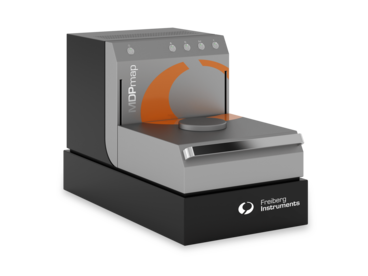
For the boron-oxygen determination a calibration factor CBO is used, which depends on the injection and doping concentration. With the MDPmap and the heated sample stage a determination of the boron-oxygen concentration is possible for mc- and mono-Si with a high resolution.
µPCD/MDP (QSS)
PID
X-ray diffraction
Projects
Company
This Website uses cookies Our website uses cookies and the web analytics tool Google Analytics according to our privacy policy. By continuing to browse these pages, you agree. If you do not want to collect data from Google Analytics, you can disable this here