Non-destructive measurements of minority carrier lifetime are well established and widely used for process control and characterization of defects in crystalline silicon. With our tool MDPinline it is possible to map the minority carrier lifetime with a so far unsurpassed combination of spatial resolution, sensitivity and measurement speed. MDP inline tools enable whole wafer maps with a resolution of 2.8 mm up to (156 x 156 mm) in less than one second
When it comes to the measurement of raw wafers it has to be taken into account, that not the actual bulk lifetime, but the effective lifetime, which consists of the surface and the bulk recombination, is measured.
Therefore the measured lifetime of an as-grown wafer with a thickness of 200 μm is limited to approximately 2.3 μs. However if the bulk lifetime is very small, it will dominate the effective lifetime, so that a low quality can be recognized. Figure 1 displays the lifetime map of an as-grown multicrystalline wafer from the edge of a cast. The low quality edge, due to the contact with the crucible, can be easily distinguished from the better parts.
Material classification
The MDP inline tool is able to classify wafers in up to 15 quality classes. For that, different characteristic parameters are taken into account, like arithmetic average, harmonic average, average according to J. Isenberg, median and standard deviation. Note that a direct correlation between the effective lifetime and the efficiency of the solar cells is not present, because of the cell process which affects single regions in ingots differently. The software equipment developed for this tool also determines a variety of process relevant parameters and low quality edge areas of the wafers. The combination of lifetime averages and standard deviation enables a very good classification of the material quality. Figure 2 showcases an exemplary classification of three wafers from the bottom, middle and top part of an ingot. It is even possible to distinguish wafers of the bottom from those of the top part of the ingot. Wafer of the bottom often have higher oxygen and defect concentration, which results in a lower average lifetime. Wafers from the top often have a low lifetime, because of metallic impurities, a high nitrogen and carbon concentration and segregations of SiC, Si3N4 and other crystallization defects.
Monitoring and recognition of crystal defects
For the monitoring and recognition of crystal defects an extensive study was carried out, where specific wafers with special defect constellations were measured. In this study characteristic results for different crystallographic defects were determined. One of the most abundant defects are Si3N4 and SiC segregates, which lead to shunts in the solar cell. In the MDP lifetime maps these defects lead to a very high inhomogeneity and a high percentage of pixels with a lifetime under 0.2 μs. The second most abundant crystal defects are microcrystalline structures in the wafer. These structures lead to a very low lifetime, together with a low inhomogeneity. In combination with a crack tester these microcrystalline wafers can be recognized and distinguished from the wafers with segregates.
Furnace monitoring
Another useful application is the monitoring of furnace properties. Complications in the growth process can be detected and furnace properties can be optimized. Figure 4 and 5 show two examples of the above mentioned possible applications.
In figure 4 the average of 5 ingots, which were grown in different furnaces, were plotted versus the ingot height. It becomes obvious, that different furnace properties lead to different slopes in the bottom and top part of the ingots. For example furnace 2 and 5 differ by about 30 % in the bottom slope and furnace 2 and 4 by about 50 % in the top slope. With this information an optimization of the furnace is possible.
Figure 5 displays the abundance of a crystallographic parameter, which is characteristic for the material quality. A high value indicates a low quality and vice versa. The abundance of this parameter is displayed for the wafers of different weeks of production. Several thousand wafers were analyzed. Week 4 shows a higher percentage of wafers with a high crystallographic parameter. Apparently there have been contaminations in the feedstock or something influences the growth process, which can be detected with the MDP measurements. In such a way problems can be traced back to their origin and thus can be eliminated efficiently.
Further applications especially for ingots are shown in other case studies.
Inline mappings of as-grown wafers and ingots are a versatile tool for the detection of e.g. crystallization defects early in the production process. With the MDP tools MDPingot and MDPinline a full electrical wafer characterization at up to one wafer per second is possible. Along with the effective minority carrier lifetime also the resistivity is measured. With these investigations of each individual wafer, a huge variety of applications are possible like process control, yield and process improvement as well as a fast ramping up of any new production line or process. In inline applications, this opens an entire spectrum of new possibilities towards a highly efficient optimization of products and production processes together with an improvement of yield.
For more information read:
[1] K.Dornich, N.Schüler, D. Mittelstrass, A. Krause, B. Gründig-Wendrock, K.Niemietz, J.R. Niklas, Conferenceproceedings 24th PVSEC Hamburg (2009) in press
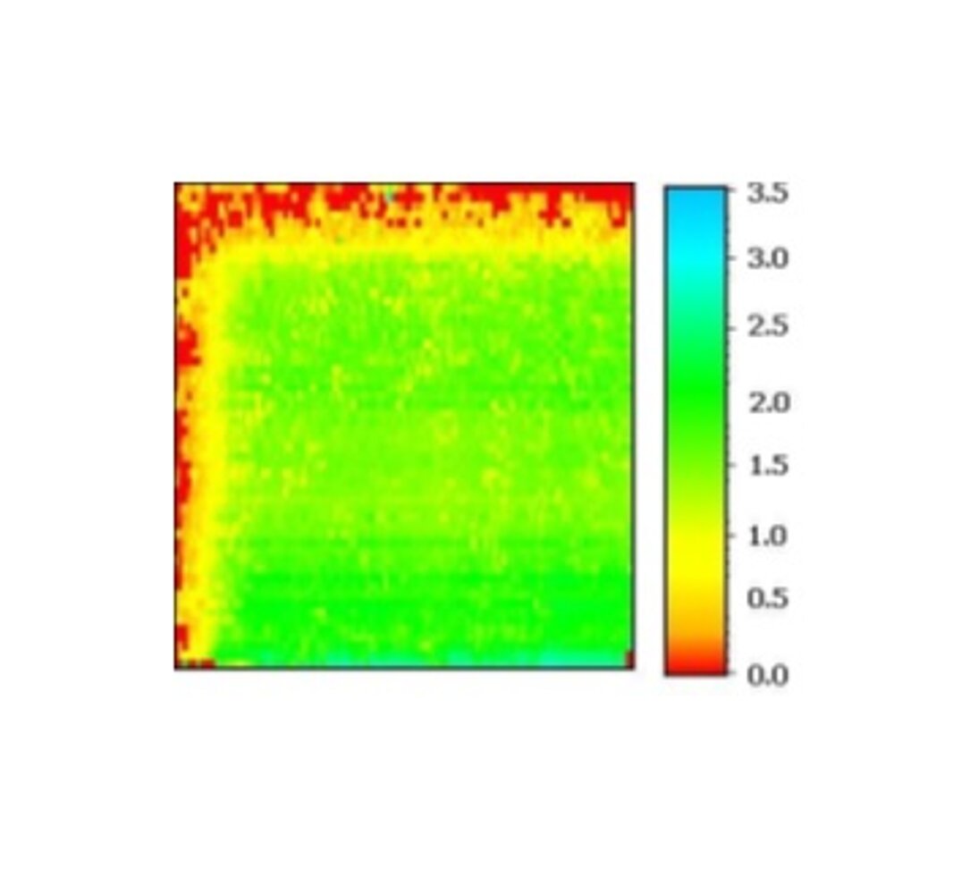
Lifetime map of a mc-Si wafer from the edge of a cast ingot
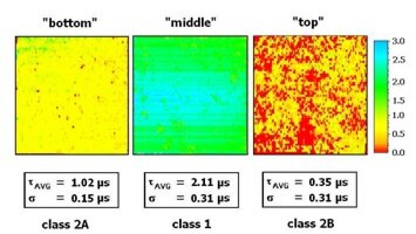
Exemplary classification of three wafers of bottom (a), the middle (b) and top(c) of an ingot.

Si3N4 and SiC segregates (a); microcrystalline wafer (b)
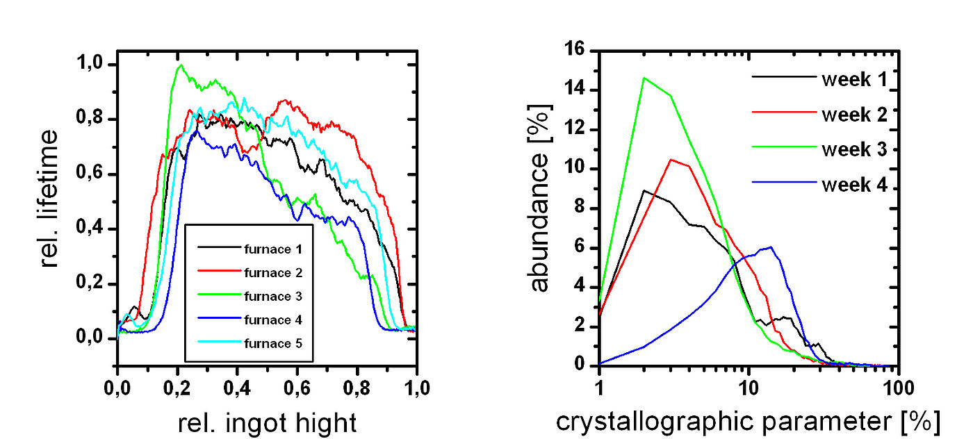
average versus ingot height for 5 ingots grown in different furnaces | histogram of the crystallographic parameter of different weeks
Related Solutions and Industries: Epitaxial Layers & Thin Films