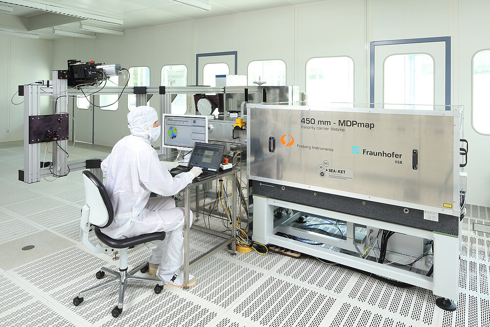
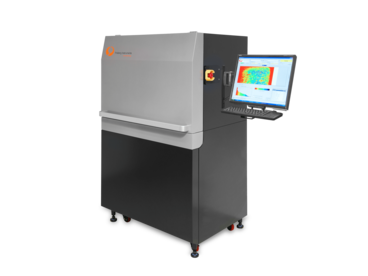
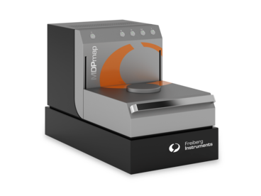
Since several years, the microelectronic industry is planning to enlarge the wafer size from 300 mm (12 inch) to 450 mm (18 inch) diameter, in order to gain more yield. The technology for the production of such high-quality wafers is now available and only the cost issue of adapting the fabs is still prohibiting the transfer to a larger wafer size. These 450 mm wafers also need to be checked for extrinsic and intrinsic impurities and hence highly spatially resolved lifetime measurements are needed. In cooperation with Fraunhofer IISB, Freiberg Instruments developed a tool for the minority carrier lifetime measurement of 450 mm wafers in the EC-funded project SEA4KET.
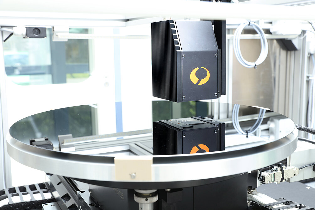
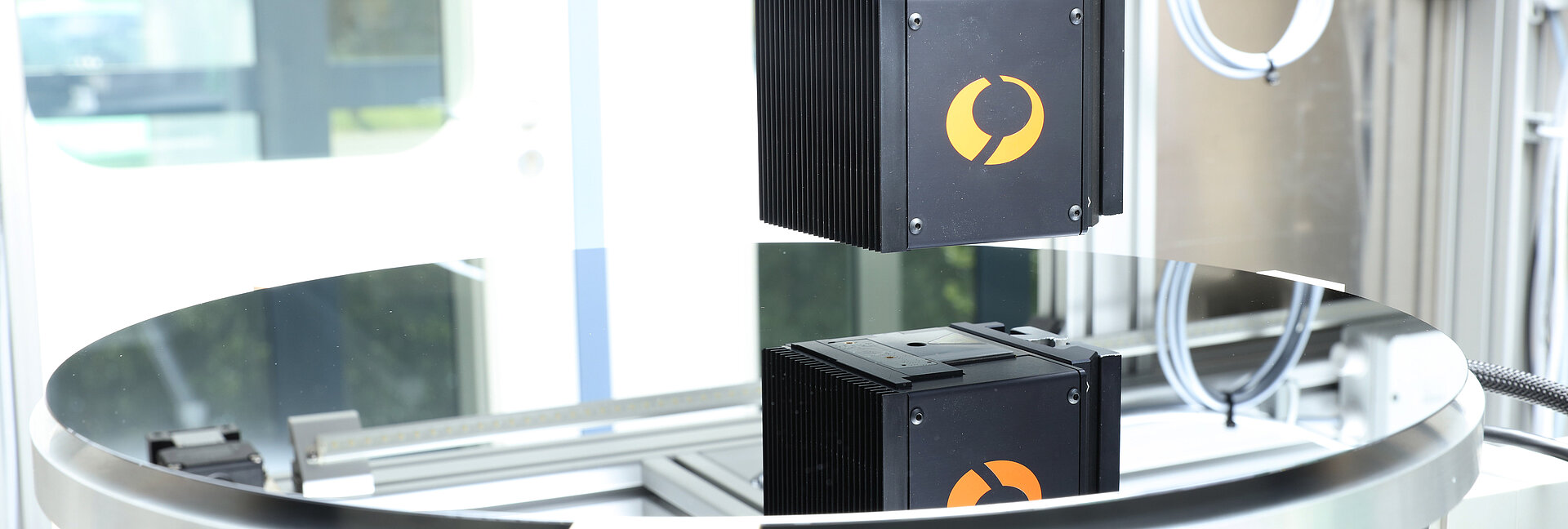
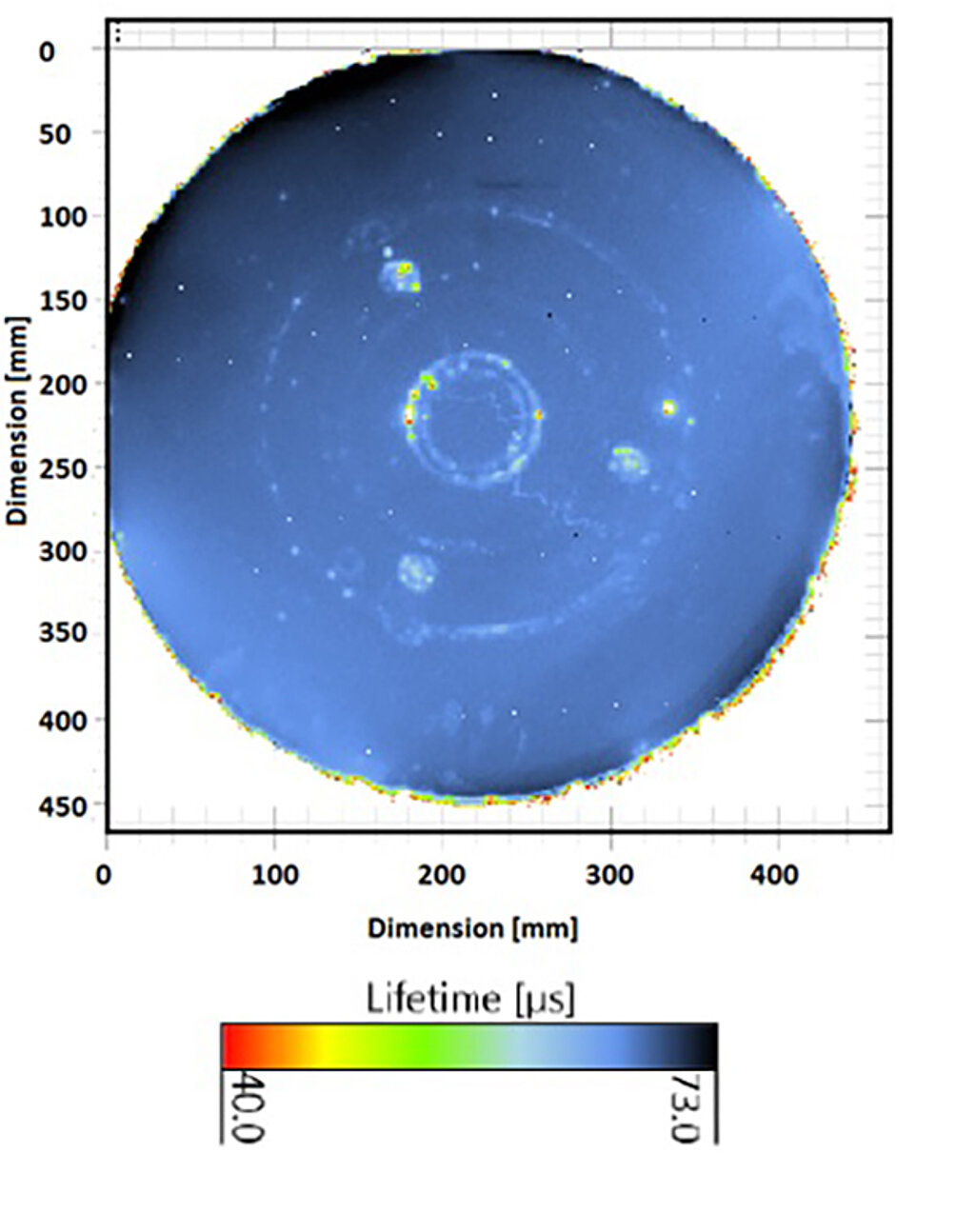
For the minority carrier lifetime measurement of 450 mm wafers basically the same measurement head as in the MDPmap and MDPpro is used with some adaption for the larger wafer size in the mapping part of the tool. Figure 1 shows one of the first measured lifetime maps of a 450 mm wafer, which clearly shows some handling traces and striations. In figure 2 and 3 the tool, which is situated in the clean room at Fraunhofer IISB is displayed.
