In the PV industry sometimes also low quality material with a high phosphorous concentration is used. Phosphor has a segregation coefficient of 0.35 and is therefore segregating in the top of the brick (last part that solidifies).There the concentration can be so high, that even changes in the conduction type from p to n can occur. Of course the n-type material cannot be used anymore for the solar cell production. Before the conduction type changes completely to n-conductivity, there is a narrow part of the ingot that is highly compensated and has a very high resistivity. Since resistivity measurements by eddy current are difficult to achieve in high resolution, it is preferable to use the photoconductivity for the detection of such a pn change.
The photoconductivity or signal height depends on the resistivity because the skin depth of the microwave increases with increasing resistivity, so that at high resistivities a larger volume of the sample is measured. This dependency can be used for the pn detection.
With a clever computer algorithm, it is possible to detect the sharp rise in photoconductivity, so that a pn-change can be detected with a resolution of 1 mm (fig.1 and fig.2). This algorithm can be implanted into the software of the MDPingot and MDPingot inline tool.
The MDPingot and MDPingot inline allows to detect pn-changes inline with a resolution of 1mm as demonstrated in figure 1 and 2. With this feature useless n-material can be sorted out as early as possible in the production process.
For more information please read:
[1] N. Schüler, D. Mittelstrass, K. Dornich, J.R. Niklas, 35th IEEE Photovoltaic Specialists Conference Honululu, (2010) 852-857
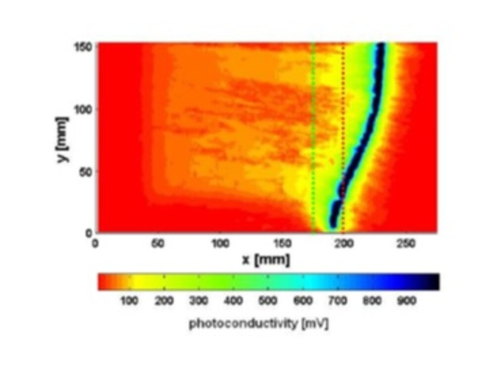
Fig. 1: photoconductivity map of a mc-Si brick with the indicated detection brick height of the pn algorithm and height at which the mean resistivity linescan rises above 3 cm
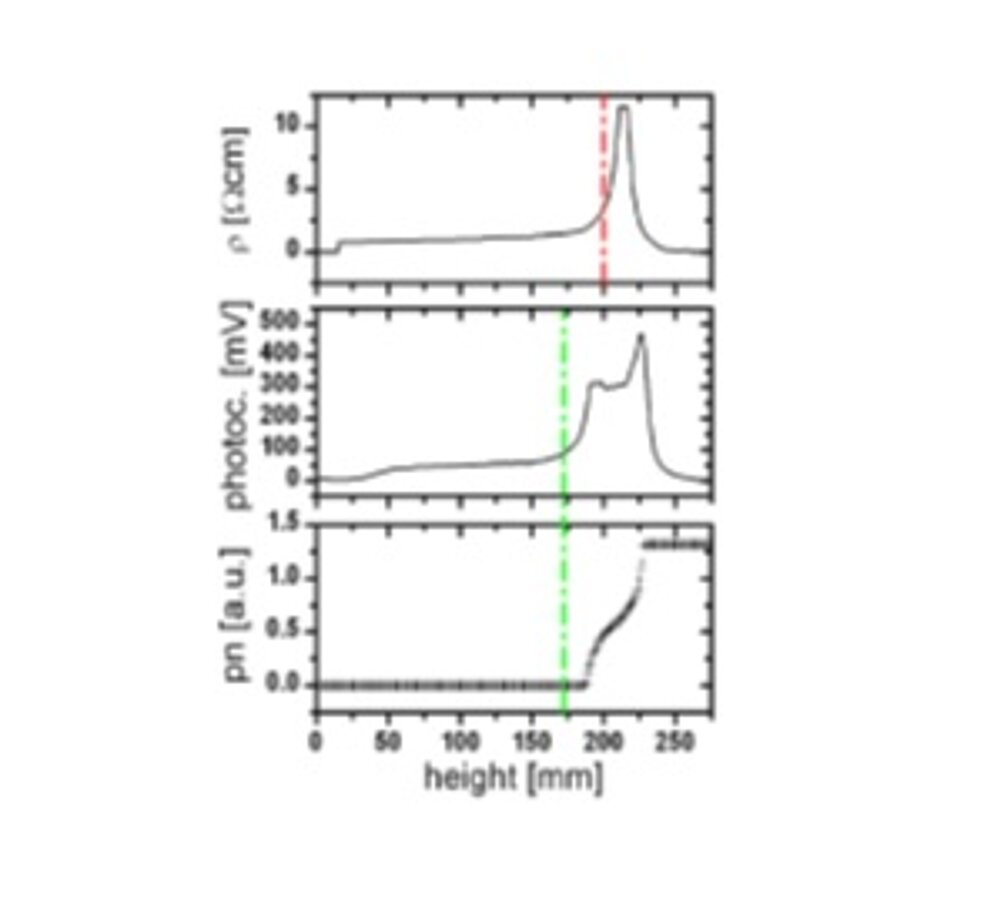
Fig. 2: mean photoconductivity linescan along with the output of the pn detection algorithm and the mean resistivity linescan
Related Solutions and Industries: Epitaxial Layers & Thin Films