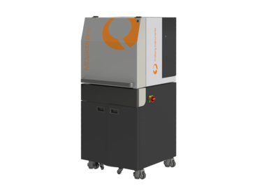
Minority carrier lifetime
The minority carrier lifetime is one of the most important and significant material parameters. It is extremely sensitive to smallest amounts of impurities or intrinsic defects and hence an ideal parameter for inline characterization of material quality and process control. It is of essential importance for the performance of many semiconductor devices. The minority carrier lifetime is defined as the average time it takes an excess minority carrier to recombine. It is strongly dependent on the magnitude and type of recombination processes in the semiconductor.
The main different types of recombination are:
SRH recombination ⇒ via defects
Auger recombination ⇒ via a three particle process
intrinsic or radiative recombination ⇒ via band to band
\(\cfrac{1}{\tau_{bulk}} =\cfrac{1}{\tau_{SRH}} + \cfrac{1}{\tau_{Auger}} + \cfrac{1}{\tau_{rad}}\)
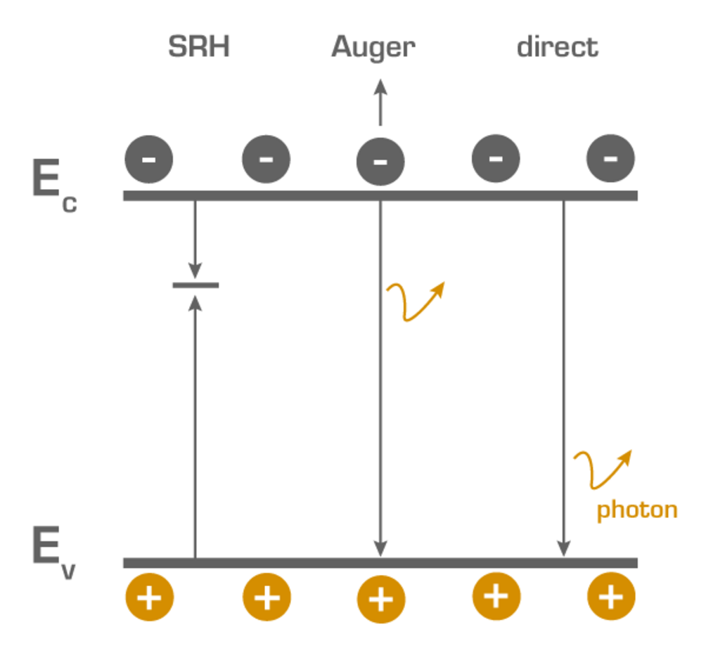
For silicon SRH is often the dominant recombination mechanism. The minority carrier lifetime in the bulk depends accordingly on the number of defects present and on their recombination properties. In silicon the lifetime can be as high as 1ms, where as in a direct semiconductor as GaAs, where the intrinsic recombination is dominant, the lifetime is only in the range of ns...µs. Besides the defect properties the minority carrier lifetime is dependent on the injection level (excess carrier concentration) and the doping concentration. Figure 1 and 2 display this dependencies for all different lifetimes.

Fig. 2: injection dependence of all important recombination rates
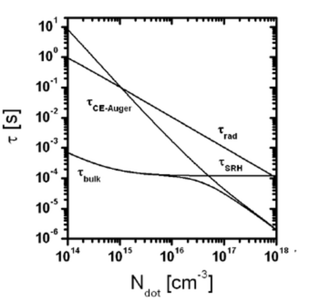
Fig. 3: doping dependence of all important recombination rates
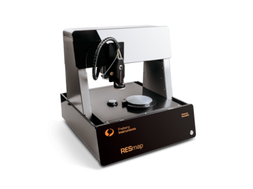
The measured effective lifetime is composed of the bulk lifetime and surface lifetime, which depends on the surface properties of a sample. Hence the surface has to be passivated, if you want to measure the bulk properties of your sample. If you want to investigate the surface passivation quality a FZ-Si wafer is recommendable, because the bulk recombination can be neglected.
\(\cfrac{1}{\tau_{eff}} = \cfrac{1}{\tau_{bulk}} + \cfrac{1}{\tau_{surface}}\)
Besides that the measured effective lifetime is dependent on the measuring method. For more details read:
[1] S. Rein, Lifetime Spectroscopy - A Method of Defect Characterization in Silicon for Photovoltaic Applications, Vol. 85 (Springer, Berlin Heidelberg, 2005)
[2] D. K. Schroder, Semiconductor Material and Device Characterization, 2 ed. (John Wiley & Sons, New York, 1998)