Generalized rate equations for lifetime simulations
This numerical tool is based on a generalized rate equation system, which is solved for all possible transitions between the defect levels in the forbidden gap and the bands of a semiconductor. The only approximation is, that no interactions between defect levels are included. This is a valid approximation, since the defect density in silicon is typically low.
The applied rate equation system describes the time dependent change of carrier concentrations in the conduction and valence band, as well as in defect levels. In this equation system the optical and thermal generation rates, the band to band and Auger recombination rates and the carrier capture and emission rates from all defects (Cj, Dj, Ej, Fj) are included. The transition rates are described without any approximations.
\(\dot{n} = G^0_{BB} + G^th_{BB} + \sum_{j}(C_j - D_j) - R_{BB} - R_{Aug}\)
\(\dot{p} = G^0_{BB} + G^th_{BB} + \sum_{j}(F_j - E_j) - R_{BB} - R_{Aug}\)
\(\dot{n}_{Tj} = D_j + E_j) - C_j - F_j\)
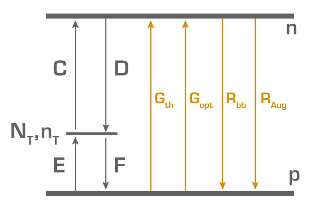
Fig. 1: energy scheme of all transition rates that are included into the simulations
From the simulated time dependent carrier concentrations the photoconductivity can be calculated using the mobility model of DORKEL and LETURCQ [2] . The minority carrier lifetime can be extracted from the transient of the photoconductivity after Gopt is set to zero.
advantages compared to SRH simulations or PC1D
lifetime is not a parameter, but a direct result
non steady state can be simulated as well
an arbitrary number j of defect levels can be included
The numerical simulation tool is suited for simulation of injection and temperature dependent measurements, for investigating the trapping effect on lifetime and photoconductivity and for the comparison of MDP and µPCD or other measurement conditions. Summarizing, this simulation tool enables to make lifetime measurements more comparable and to achieve a better understanding of the results.
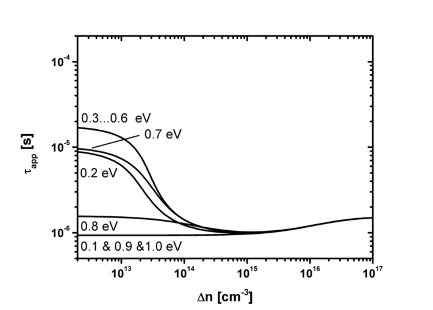
Fig. 2: varying Et
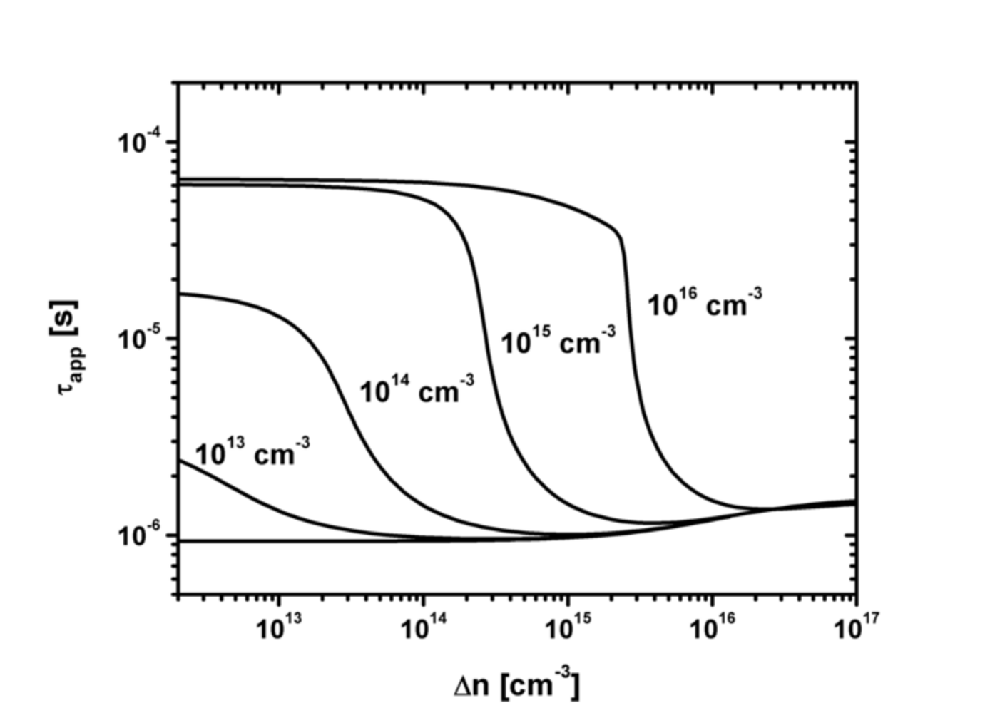
Fig. 3: varying Nt
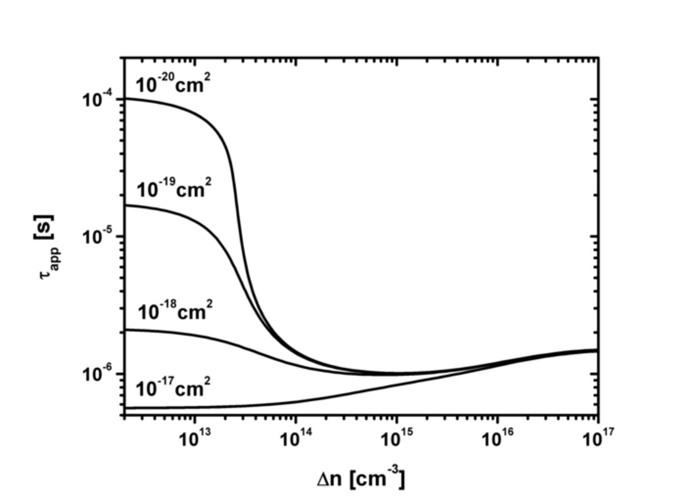
Fig. 4: varying σp
More information about these simulations can be found in:
[1] T. Hahn, Thesis, TU Bergakademie, 2009
[2] J. M. Dorkel and P. Leturcq, Solid-State Electronics 24, 821-825 (1981)