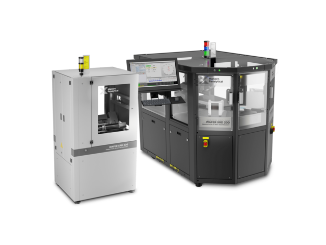
Materials
With Wafer XRD, a wide variety of materials can be precisely analyzed. Thanks to their flexibility and performance, our systems meet even the most demanding requirements.
Si SiC Quartz GaN GaAs AIN InP Al₂O₃ (sapphire) and more
Features & Benefits
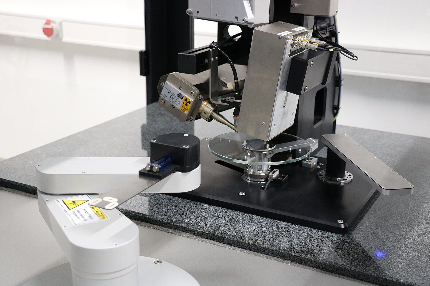
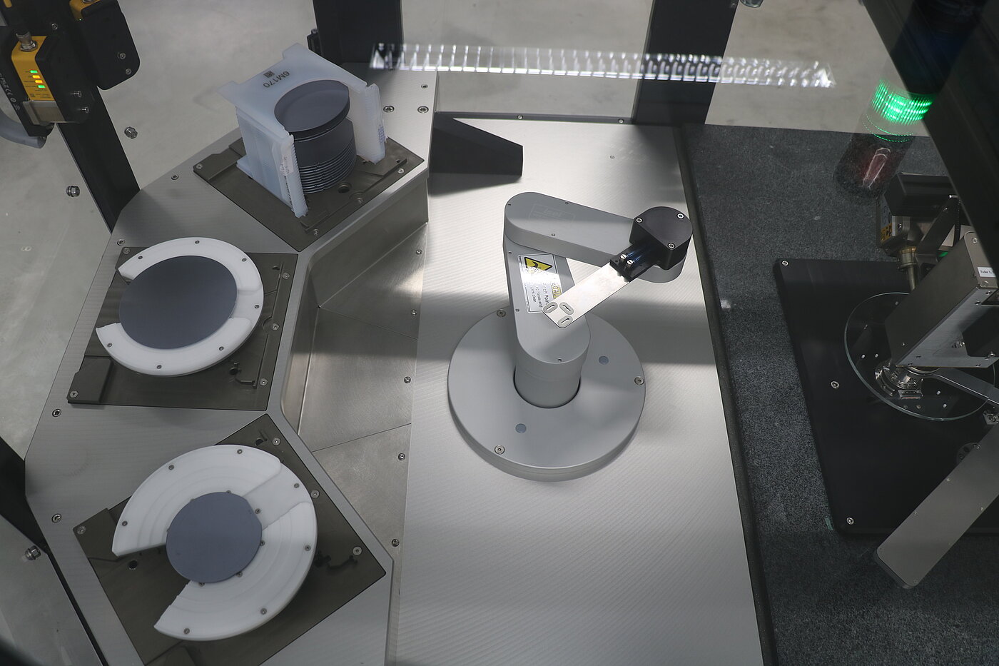
Fully automated wafer sorting and handling system


