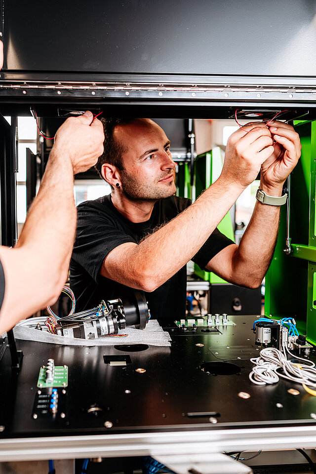
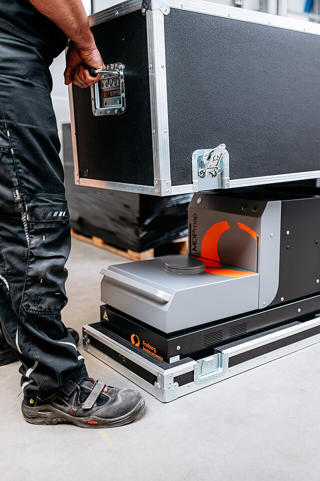
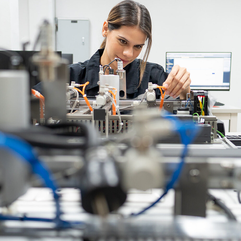
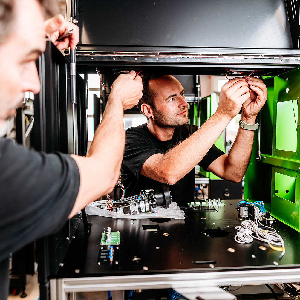
Bringing Innovation from Lab to Fab
At Freiberg Instruments, we drive technological advancements by developing high-precision measurement and automation solutions that set new industry benchmarks. Our systems enable leading companies and researchers to enhance their processes and gain reliable data for breakthrough innovations.
With over 3,000 metrology systems installed worldwide, we serve industries such as microelectronics, semiconductors, photovoltaics, chemicals, and medical technology. Our dedication to quality—certified according to ISO 9001:2015 – makes us a trusted partner for future-driven solutions.
Our goal: transforming innovation from the lab into industrial applications—efficiently, precisely, and sustainably.
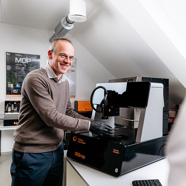
Cutting-edge Metrology Solutions for Various Applications

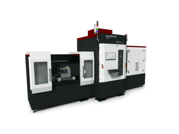
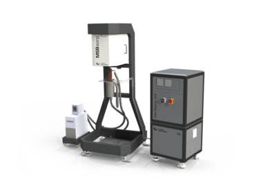
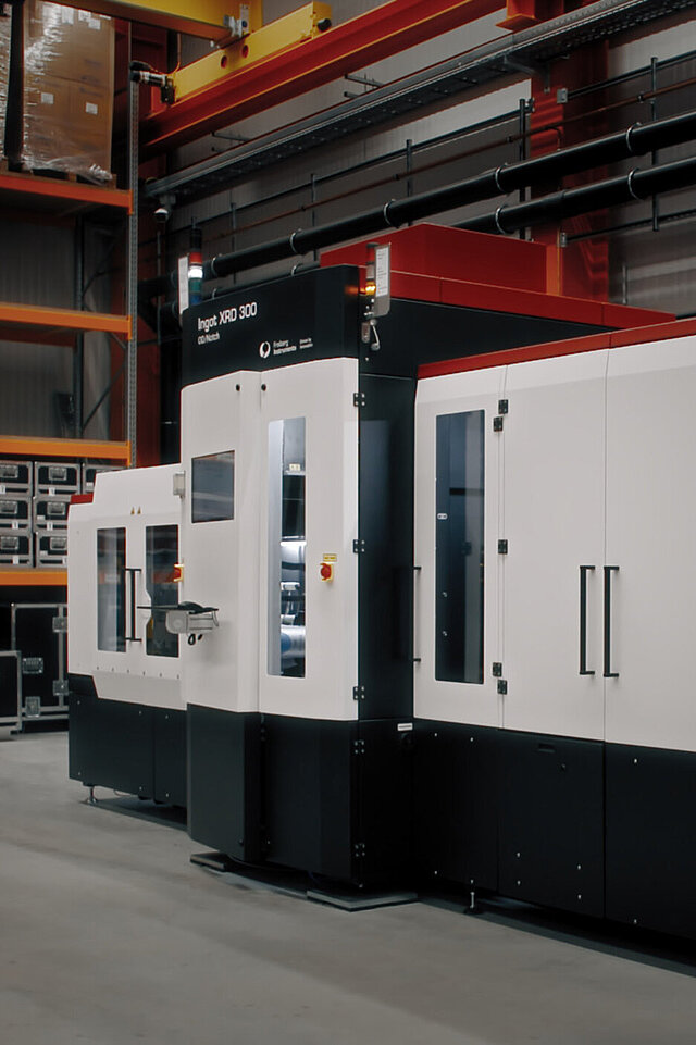
Our advanced X-ray diffraction (XRD) systems optimize grinding and sawing processes, ensuring perfect alignment for high-performance semiconductor applications.
Discover more
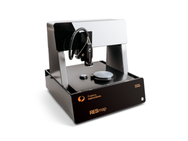
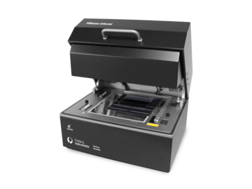
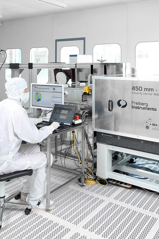
Our non-destructive metrology tools provide critical insights into wafer properties, layer thickness, and defect detection.
Discover more
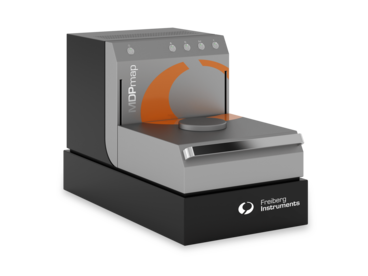
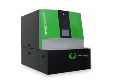
Our advanced tools support high-speed, high-accuracy analysis of wafers and thin films, ensuring optimal yield and production performance.
Discover more
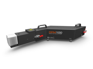
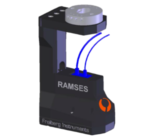
Our instruments provide unparalleled sensitivity and reliability in geochronology and dosimetry applications.
Discover more
Our solutions provide real-time monitoring, ensuring compliance and protection in critical industrial and research environments.
Discover more
Our advanced metrology tools support material research, semiconductor development, and defect analysis with maximum accuracy.
Discover morePrecision Redefined: Discover Our Advanced Metrology and Automation Solutions

We are driven by Innovation. Freiberg Instruments constantly redefines the limits. Excellence in Automation and Metrology is our core motivation.
Dr. Kay Dornich
CEO
Stay Connected on LinkedIn
Follow Freiberg Instruments on LinkedIn for weekly updates, exclusive product showcases, and industry insights. Join our community to stay informed about the latest innovations and milestones shaping the future of automation and metrology. Don’t miss out – be part of the conversation!

Driving Innovation
with You
Our team of engineers, scientists, and professionals shares a relentless passion for excellence. Together, we have built a reputation for reliability, innovation, and exceptional customer service. We constantly redefines the limits of metrology.
Discover more
About Freiberg Instruments

