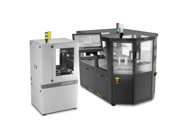
High-Precision Wafer Testing with Omega-Scan
To ensure the exceptional performance required for semiconductors, every wafer must undergo thorough testing. The Omega-Scan method, known for its speed and precision, is ideal for fully automated in-line X-ray diffraction (XRD) solutions. It enables comprehensive surface characterization, including surface tilt vector analysis and in-plane direction measurement—such as perpendicular alignment to the wafer flat. Additionally, it provides automated detection of wafer flats or notches along with their precise measurements.
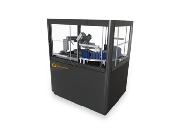
Omega-Scan solutions are available for all standard wafer materials and orientations. Quartz remains the most commonly used material, where integrating mapping technology proves especially beneficial. By identifying high-quality wafer regions before cutting blanks, the process ensures optimal material utilization. During wafer production, heat-induced stress can cause bending, leading to warp and bow. See Fig 1 & 2. An optional sensor accurately measures these deformations, ensuring precise quality control.

Fig. 1 - Warp and bow measument with a line laser instrument attached to the diffractometer
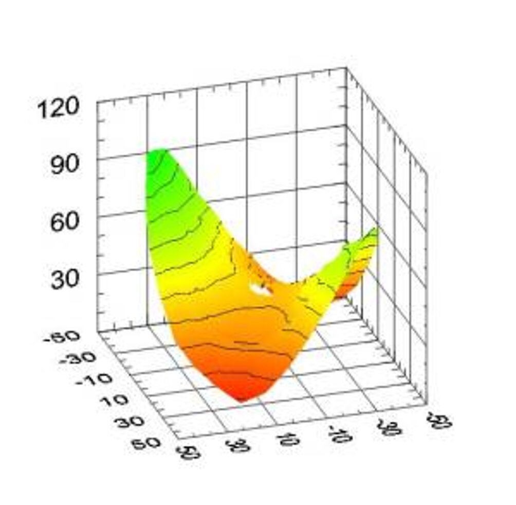
Fig. 2 - Sapphire wafer surface geometry as the result of the warp and bow measurement
Related Technologies: Omega-scan, Theta-scan
Related Solutions and Industries: Epitaxial Layers & Thin Films