Found 271 results in 1 milliseconds.

Page

Projects

R&D Projects Achieving goals together: Projects with measurable added value Freiberg Instruments stands for the highest precision and groundbreaking technologies in materials research and measurement technology. Our projects impressively demonstrate how versatile and adaptable our solutions are – from collaboration with renowned research institutions to complex industrial applications . We rely on innovative approaches, tailor-made technologies and a close partnership with our customers. Whether it is about supporting groundbreaking research or increasing efficiency in production – our projects are proof of our expertise and our commitment to the highest standards. Our Research & Development Projects Electrical semiconductor characterization View projects Luminescene dating, research, dosimetry View projects Our Partners Discover More Solutions Crystal Growth and Processing Learn more Epitaxial Layers & Thin Films Learn more Photovoltaic Learn more Luminescence Dating and Dosimetry Learn more

Page

Software

Lexsyg Software LexStudio 2.0 - Operating software Modern, professionally designed user interfacensitivity: Based on user feedback a new graphical user interface which combines clear arrangement and usability is developed by Freiberg… Learn more LexEva - Evaluation software LexEva is a newly released evaluation software developed for analysis in luminescence research and dating. LexEva was adapted to the "Luminescence" package developed by the R. Luminescence… Learn more TLStudio - Operating & Evaluation software User account management system, Transperent workflow, Professionally designed user interface, Intelligent parameter selection, Live data visualization, Easy programming of individual and… Learn more OSLdosimetry OSLdosimetry is a user friendly operating software which allows OSL dose measurements as standard user or calibration and setting features for professionals (password protected). The… Learn more

Page

Applications

Lexsyg Applications Radiation protection dosimetry TL, OSL, Radioluminescence, Electron Spin Resonance (ESR), Neutron dosimetry, Food irradiation and clinical dosimetry Thermoluminescence (TL) Learn more Photo/ Optically Stimulated Luminescence (PSL + OSL) Learn more Radioluminescence Learn more Electron Spin Resonance (ESR) Learn more Neutron dosimetry Learn more Food Irradiation Control Learn more Medical dosimetry Learn more Solid state dosimetry Luminescence spectroscopy, Time resolved luminescence, Spatially resolved luminescence and Electron Spin Resonance (ESR) Luminescence spectroscopy Learn more Spatially resolved luminescence Learn more Time resolved luminescence Learn more Electron Spin Resonance (ESR) Learn more Geology OSL, IRSL, Single grain/spatially resolved luminescence, Radiofluorescence, Electron Spin Resonance (ESR) and Pulsing Optically stimulated Luminescence dating of quartz (OSL) Learn more Infrared stimulated Luminescence dating of feldspar (IRSL) Learn more Single grain/spatially resolved luminescence dating Learn more Radiofluorescence Learn more Electron Spin Resonance (ESR) dating of quartz Learn more Pulsing: mixed mineral samples Learn more Archaeology Luminescence methods provide the age of archaeological sites or objects Flint and other heated rocks Learn more Ceramics, pottery, bricks and statues Learn more Unheated rock surfaces Learn more Tooth enamel and quartz grains Learn more Sediment dating Learn more

Technology

PIDStudio

PIDStudio User friendly and advanced operating software PIDStudio is a cutting-edge, user-friendly software that is continuously updated and improved based on user feedback. It allows for easy handling and provides intuitive functionality. With PIDStudio , you can output and compare key parameters from multiple measurements, including: Parallel Resistance Conductance Power Loss Leakage Current Temperature Humidity High Voltage Key Features: User-friendly interface Export functionality Customizable recipes Pass/fail criteria Comprehensive analysis tools Control of multiple devices This software is designed to simplify and enhance the PID testing process. Get in touch Do not hesitate to contact us – we are available to assist you with any inquiries or requests. Use our inquiry tool or reach out via email: sales @ freiberginstruments.com
Product

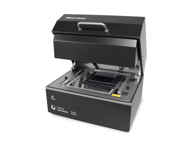
PIDcon bifacial

Skip breadcrumb navigation Breadcrumb Freiberg Instruments Products Potential Induced Degradation PIDcon bifacial PID con bifacial Quality Control Solution for Bifacial PERC/PERC+, HIT, Topcon, c-Si Solar Cells, Mini Modules, and More Interested? Get in touch! Contact now Product Sheet Skip menu Quick navigation Features Applications Specifications Technology Contact Benchtop PID tester for c-Si solar cells and mini-modules PID detection at cell level Research, Production & Quality Control of PERC, AL-BSF, PERC+, bifacial PERC, PERT, PERL and IBC solar cells No climate chamber necessary Features & Benefits Measurements of cells Test duration: 4 hours (typical) Voltage: ± 1.5 kV Module vs. Cell level PID test Applications Production Monitoring Potential Induced Degradation (PID) is a significant reliability issue in photovoltaic (PV) power plants. It is crucial to assess the susceptibility of products to PID early in the production… Learn more EVA Evaluation The PIDcon allows for the investigation of how EVA foil affects PID susceptibility using a sample stack that simulates a module. To perform the test, the user simply places a solar cell, the EVA… Learn more Solar Cell Classification Potential Induced Degradation (PID) poses a significant reliability issue in PV power plants, making it essential to assess products for their susceptibility to PID. The PIDcon system enables… Learn more Mini-module Classification Potential Induced Degradation (PID) is a critical reliability issue in PV power plants, making it essential to assess products for their susceptibility to PID. The PIDcon system helps… Learn more Glass Evaluation For more information please read:[1] V. Naumann, Ursachenanalyse und physikalische Modellbildung für potenzial-induzierte Degradation von Silizium-Solarzellen, Dissertation,… Learn more With our PIDcon bifacial testing device, module manufacturers can perform reliable quick tests of solar cells and encapsulation materials during production. Dr. Christian Hagendorf Key Account Manager Interested? Our experts are happy to assist you. Get in touch! Contact us now! Specifications Type Stress Recovery PID-s front 85 °C, +1.5 kV 85 °C, -1.5 kV PID-p rear 85 °C, +1.5 kV, without illumination 85 °C, dark storage or illumination PID-c rear 85 °C, +1.5 kV, with illumination Not possible Lamination 150 °C, 20 min Sample size up to 210 x 210 mm Suitable for For PERC, AL-BSF, IBC, PERC+, bifacial PERC p- and n-type Measurement of Measurement of: R parallel , leakage current, IV curve under illumination Download Product Sheet PDF (640 KB) Technologies Physical Nature of PID-s In the field a large potential between the front glass surface and the solar cells in a module can occur and a shunting of the p-n junction of a Si solar cell and accordingly a decrease in… Learn more Comparison of PID Test Methods The PIDcon test has the following advantages compared to other methods:Short duration (usually 4–8h), High variability: test of solar cell, mini-module, glass and EVA, Good control of test… Learn more Dependencies of PID Susceptibility For more information please read:[1] V. Naumann, Ursachenanalyse und physikalische Modellbildung für potenzial-induzierte Degradation von Silizium-Solarzellen, Dissertation,… Learn more Conductance Test and Power Loss Furthermore an easy pass or fail criterion after finishing the PID measurement is suggested. It is assumed that an efficiency loss of 3% at the end of the PID test lead to a fail of the solar… Learn more Get in touch Do not hesitate to contact us – we are available to assist you with any inquiries or requests. Use our inquiry tool or reach out via email: sales @ freiberginstruments.com

Page

Publications

Publications for PID B. Durusoy, D. Adner, C. Hagendorf, K. Wojciechowski, S. Almosni, M. Turek. Standardized Test Routined for the Assessment of Potential Induced Degradation of Perovskite Solar Cells K. Sporleder et al., Quick test for reversible and irreversible PID of bifacial PERC solar cells V. Naumann et al., The role of stacking faults for the formation of shunts during potential induced degradation (PID) of crystalline Si solar cells, Phys. Stat. Solidi RRL 7, No. 5 (2013) 315-318 P. Hacke et al., Proc. Of 25th EUPVSC Valencia, Spain (2010) S. Pingel et al. Proc. Of 35th IEEE PVSC, Honululu, USA (2010) V. Naumann et al., Solar Energy Materials and Solar Cells Vol. 120 (2014), 383-389 V. Naumann et al., On the discrepancy between leakage currents and potential induced degradation of crystalline silicon modules, Proc. 28th PVSEC (2013), 2994-2997 V. Naumann et al., Potential-Induced Degradation at Interdigitated Back Contact Solar Cells, Energy Procedia (2014)

Page

Technology

PID Technology Physical Nature of PID-s In the field a large potential between the front glass surface and the solar cells in a module can occur and a shunting of the p-n junction of a Si solar cell and accordingly a decrease in… Learn more Comparison of PID Test Methods The PIDcon test has the following advantages compared to other methods:Short duration (usually 4–8h), High variability: test of solar cell, mini-module, glass and EVA, Good control of test… Learn more Dependencies of PID Susceptibility For more information please read:[1] V. Naumann, Ursachenanalyse und physikalische Modellbildung für potenzial-induzierte Degradation von Silizium-Solarzellen, Dissertation,… Learn more Conductance Test and Power Loss Furthermore an easy pass or fail criterion after finishing the PID measurement is suggested. It is assumed that an efficiency loss of 3% at the end of the PID test lead to a fail of the solar… Learn more

Page

Applications

PID Applications Production Monitoring Learn more EVA Evaluation Learn more Solar Cell Classification Learn more Mini-module Classification Learn more Glass Evaluation Learn more

Application

Contactless detection of bulk polarization phenomena in semiconductors

Contactless detection of bulk polarization phenomena in semiconductors Aim Characterization of bulk polarization phenomena such as the bulk photo-voltaic effect (BPVE) in semiconductors requires the preparation of two electrical contacts on the sample, which inevitably introduces additional defects in the semiconductor-metal interface what is especially challenging for ultrawide bandgap semiconductors with high resistivity. Solution Surface photovoltage (SPV) spectroscopy using a Kelvin probe is used as a nondestructive, contactless method for characterizing the change of the contact potential difference (DCPD) in carbon doped GaN single crystals. By designing a unique setup capable of measuring DCPD up to ± 200 V, large photovoltages could be detected, without the need to deposit electrical contacts. Application example The band gap of GaN is 3.4 eV. As an example, figure 1 shows a spectrum of DCPD for a carbon doped GaN crystal (GaN:C). The corresponding SPV signal reached more than 13 V at 3 eV, i.e., under excitation of certain defect states, SPV signals were much larger than expected from the band gap (for more details see [1]). A change of the direction of DCPD and a signature in the derivative were found near the band gap. Under excitation with a laser diode (445 nm) at higher intensity, the maximum signal was obtained for GaN:C with a carbon concentration of 9×10 18 cm -3 and amounted to about 23 V, far exceeding the band gap (figure 2). Fig.1: Spectra of DCPD and its deriva-tive for a GaN:C crystal. SPV signals are much larger than the band gap for excita-tion in the defect range (data after [1]). Fig. 2: Time dependence of DCPD of a GaN:C crystal measured during illumination with a laser diode at 445 nm and after switching off illumination. References [1] Levine, I., et al. "Bulk photovoltaic effect in carbon-doped gallium nitride revealed by anomalous surface photovoltage spectroscopy." Phys. Rev. B 101 (2020) 245205. Related Solutions and Industries: Epitaxial Layers & Thin Films Matching Products SPS/SPV series HR-SPSmap with fixed energy excitation sources High-Resolution and Sensitive Surface Photovoltage Measurement Solutions Learn more SPS/SPV series HR-SPSmap with variable energy excitation source with a variable energy excitation source Learn more Get in touch Do not hesitate to contact us – we are available to assist you with any inquiries or requests. Use our inquiry tool or reach out via email: sales @ freiberginstruments.com

Application

Electronic transitions in diamond

Electronic transitions in diamond Aim For further development of optoelectronic devices and other applications based on diamond and nanodiamond, contactless characterization of electronic defect states and electronic transitions in bulk diamond and at diamond surfaces over a wide spectral range is of great interest. Solution Contactless surface photovoltage (SPV) spectroscopy in the Kelvin probe (direct measurement of the contact potential difference, DCPD) and modulated regimes provides information about transitions energies and direction of charge separation in a spectral range from near infrared (< 0.5 eV) up to the deep ultraviolet (> 6 eV) at high sensitivity. Application example Diamond has an ultra-wide indirect band gap of 5.47 eV [1]. Figure 1 shows the DCPD spectrum and its derivative for a polycrystalline diamond sample prepared by CVD. Transitions related to excitation via defect states and transitions around the band gap can be clearly distinguished [2]. For the modulated SPV spectra of another diamond sample, the sensitivity is increased and transitions at 5.258 and 5.544 eV related to absorption assisted by the indirect exciton and transversal optical phonon are well pronounced. Related spectra are like fingerprints and can be used, for example, for inline control in production lines. References [1] C. D. Clark, P. J. Dean, P. V. Harris, “Intrinsic edge absorption in diamond”, Proc. R. Soc. London A 277, 312 (1964). [2] Th. Dittrich and S. Fengler, “Transitions in polycrystalline diamond probed by surface photovoltage spectroscopy”, to be submitted. Figure 1: Spectra of DCPD and its deriva-tive for polycrystalline CVD diamond (data after [2]). Onsets at major defect transitions and around the band gap. Fig. 2: In-phase and phase-shifted by 90° modulated SPV spectra of a diamond crystal. Dotted lines give defect related transitions and transitions Eg - Ex ± hvTO. Related Solutions and Industries: Epitaxial Layers & Thin Films Matching Products SPS/SPV series HR-SPSmap with fixed energy excitation sources High-Resolution and Sensitive Surface Photovoltage Measurement Solutions Learn more SPS/SPV series HR-SPSmap with variable energy excitation source with a variable energy excitation source Learn more Get in touch Do not hesitate to contact us – we are available to assist you with any inquiries or requests. Use our inquiry tool or reach out via email: sales @ freiberginstruments.com