Found 271 results in 3 milliseconds.

Application

Light Beam Induced Current (LBIC)

Light Beam Induced Current (LBIC) Light Beam Induced Current (LBIC) is a primarily in the photovoltaic sector well established method for the spatial resolved measurement of recombination active defects in ready-progressed solar cells. The proceeding is based on the measurement of the local short circuit current Isc in the cell, which is produced through appropriate excitation. For the measurement the solar cell is contacted and locally irradiated with laser light. Advantages are the simple buildup and the high resolution, disadvantage is the exigency of contacting the sample, for which reason only ready-progressed cells can be examined. Predictions about lifetime, mobility or defect details are possible. From the measured short circuit current the external quantum efficiency can be determined via: \(EQE = \cfrac{I_{SC}\cdot h \cfrac{c}{\lambda}}{P \cdot e}\) where P is the laser power and l the wavelength. The external quantum efficiency depends on the properties of the cell volume but also on the reflection properties of the surface. If the reflection can be neglected the following mechanism determines the EQE: recombination of minority carriers in the volume recombination of minority carriers at the surfaces at the front and the back shunts in the solar cell The internal quantum efficiency IQE includes the reflection of the light at the surface: \(IQE = EQE\cfrac{1}{1 - R(\lambda)}\) In order to determine the diffusion length, it is necessary to measure IQE for at least 4 different wavelengths, which should differ in the penetration depth. The slope of 1/IQE vs. 1/a is the reciprocal of the effective diffusion length. Fig. 1: internal quantum efficiency of a solar cell measured with 4 different wavelength Related Solutions and Industries: Epitaxial Layers & Thin Films , Photovoltaic Matching Products MDP series MDpicts pro High-Resolution, Temperature-Dependent Lifetime Measurement System for Precise Material Characterization Learn more MDP series MDPpro 850+ Advanced Solution for Quality Control of Monocrystalline Silicon Ingots, Bricks, and Wafers Learn more MDP series MDPpro Advanced Lifetime Measurement System for Quality Control and Material R&D on Semiconductors Learn more MDP series MDPmap Precision Lifetime Charachterization with Exceptional Sensitivity Learn more Get in touch Do not hesitate to contact us – we are available to assist you with any inquiries or requests. Use our inquiry tool or reach out via email: sales @ freiberginstruments.com

Application

Resistance measurements on wafers and bricks

Resistance measurements on wafers and bricks The resistivity is one of the most important electrical parameters of a material. It is a key parameter for the performance of semiconductor devices as e.g. solar cells and depends on the doping density of the material. (Alttext Kürzen) With MDPmap and MDPingot it is possible to measure the resistivity of wafers or bricks with a high accuracy and a resolution of 1 mm via eddy current measurements. The Eddy current sensor setup has a very good long-term stability, due to a distance correlated internal calibration matrix. Hence, with every resistivity map a geometry map of the surface flatness is measured. The resistivity can be measured simultaneously with the minority carrier lifetime and photoconductivity maps. In case of wafer measurements, the thickness of the sample has to be given by the user. Step width ≥ 1mm Edge exclusion 12 mm Resistivity wafer thickness range 150 ...250 µm Resistivity range can be specified Default setting: 0.5 to 5 Ohm cm Accuracy: < 5 % Repeatability: < 1 % (range of 0.5 until 3 Ohm cm) It is possible to map the sheet resistance of the emitter, in order to investigate the homogeneity of the emitter diffusion. The resistivity of the base has to be given by the user. Sheet resistance measurement with range 0.1-200 Ohm/sq Accuracy at standard sample size, 0.1 - 10 Ohm/sq: < 3 % accuracy 10 - 100 Ohm/sq: < 4 % accuracy 100 – 200 Ohm/sq: < 5 % accuracy Figure 1 to 3 show examples of resistivity maps measured on mc-Si wafers and bricks. Fig 1: Emitter sheet resistance map of a typical mc-Si wafer with emitter diffusion and an average sheet resistance of 85.1 Ohm/sq. Fig. 2: resistivity map of a typical mc-Si wafer for PV applications and an average resistivity of 1.0 Ohm cm Fig. 3: Resistivity map of a typical mc-Si brick for PV applications and an average resistivity of 1.4 Ohm cm Related Solutions and Industries: Epitaxial Layers & Thin Films , Photovoltaic Matching Products MDP series MDPspot Quick and Simple Lifetime Measurement Made Easy Learn more MDP series MDPpro 850+ Advanced Solution for Quality Control of Monocrystalline Silicon Ingots, Bricks, and Wafers Learn more MDP series MDPpro Advanced Lifetime Measurement System for Quality Control and Material R&D on Semiconductors Learn more MDP series MDPmap Precision Lifetime Charachterization with Exceptional Sensitivity Learn more Get in touch Do not hesitate to contact us – we are available to assist you with any inquiries or requests. Use our inquiry tool or reach out via email: sales @ freiberginstruments.com

Application

Photoconductivity measurements and trap analysis

Photoconductivity measurements and trap analysis of wide bandgap nitride semiconductors Equipped with a 355 nm laser (μ-PCD) or a 375 nm laser diode (MDP), the MDPmap as well as the MDpicts from Freiberg Instruments are suitable for photoconductivity measurements and trap analysis on wide-bandgap nitride semiconductors. The homogeneity of n-type doping can be analyzed by means of the photoconductivity (signal height). It is strongly dependent on the resistivity and the carrier lifetime. The usually long apparent lifetimes are caused by trapping centers in the samples. Deep traps in wide-bandgap semiconductors can be investigated by MDpicts in the temperature range from 30 K up to 800 K. Compared to related methods (e.g. DLTS), MDpicts is a contactless and nondestructive method which also allows the investigation of highly n-doped semiconductors. The trap activation energy can be determined from the slope of the Arrhenius plot or estimated by directly fitting the lifetime reduction as a function of temperature by τ(T)= τ 0 /((1+aexp-E A /kT)). From the value of E A ~ 1.0 eV the main defect in the unintentionally doped GaN sample (see Figure 2 left) can be assumed to be C N . Figure 1: Photoconductivity maps measured by MDP of four different Si doping concentrations in GaN layers. Figure 2: Examples of the MDpicts time constants as a function of inverse temperature for left an unintentionally doped GaN sample and right a Si-doped GaN sample. Related Solutions and Industries: Epitaxial Layers & Thin Films Matching Products MDP series MDpicts Temperature-Dependent Lifetime Measurement System for Advanced Material Analysis Learn more MDP series MDPmap Precision Lifetime Charachterization with Exceptional Sensitivity Learn more Get in touch Do not hesitate to contact us – we are available to assist you with any inquiries or requests. Use our inquiry tool or reach out via email: sales @ freiberginstruments.com

Page

Publications

Publications for MDP A.S. Kovali, M. Demant, B. Rebba, N. Schüler, J. Haunschild, S. Rein Early stage quality assessment in silicon ingots from MDP brick characterization Jan Beyer, Nadine Schüler, Jürgen Erlekampf, Birgit Kallinger, Patrick Berwian, Kay Dornich, Johannes Heitmann Minority Carrier Lifetime Measurements on 4H-SiC Epiwafers by Time-Resolved Photoluminescence and Microwave Detected Photoconductivity Paul M. Jordan, Daniel K. Simon, Franz P.G. Fengler, Thomas Mikolajick, and Ingo Dirnstorfer 2D Mapping of Chemical and Field Effect Passivation of Al 2 O 3 on Si Substrates Paul M. Jordan, Daniel K. Simon, Thomas Mikolajick, and Ingo Dirnstorfer BiasMDP: Carrier lifetime characterization technique with applied bias voltage N. Schüler, B. Berger, A. Blum, K. Dornich, J.R. Niklas High Resolution Inline Topography of Iron in P-doped Mutlicrystalline Bricks by MDP K. Dornich, N. Schüler, J.R. Niklas Injection dependent lifetime spectroscopy with a varying pulse length K. Dornich, N. Schüler, B. Berger, J.R. Niklas Fast, high resolution, inline contactless electrical semiconductor characterization for photovoltaic applications by MDP Bastian Berger, Nadine Schüler, Sabrina Anger, Bianca Gründig-Wendrock, Jürgen R. Niklas, Kay Dornich Contactless electrical defect characterization in semiconductors by microwave detected photo induced current transient spectroscopy (MD-PICTS) and microwave detected photoconductivity (MDP) N. Schüler, T. Hahn, K. Dornich and J.R. Niklas: Spatially resolved determination of trapping parameters in P-doped silicon by microwave detected photoconductivity 25th EUPVSEC Valencia, Spain N. Schüler, D. Mittelstrass, K. Dornich and J.R. Niklas: High resolution inline detection of changes in the conduction type of multicrystalline silicon by contact less photoconductivity measurements 35th IEEE Photovoltaic Specialists conference, Honolulu Hawaii N. Schüler, D. Mittelstrass, K. Dornich, J.R. Niklas and H. Neuhaus: Next generation inline minority carrier lifetime metrology on multicrystalline silicon bricks for pv 35th IEEE Photovoltaic Specialists conference, Honolulu Hawaii N. Schüler, T. Hahn, K. Dornich, J.R. Niklas: Versatile simulation tool and novel measurement method for electrical characterization of semiconductors Solid State Phenomena 156-158, 241-246 (2010) N. Schüler, T. Hahn, S. Schmerler, S. Hahn, K. Dornich and J.R. Niklas: Simulations of photoconductivity and lifetime for steady state and nonsteady state measurements Journal of Applied Physics 107 (2010), 064901 N. Schüler, T. Hahn, K. Dornich, J.R. Niklas, B. Gründig-Wendrock: Theoretical and experimental comparison of contactless lifetime measurement methods for thick silicon samples Solar Energy Materials & Solar Cells 94 (2010), 1076-1080 K. Dornich, N. Schüler, D. Mittelstraß, A. Krause, B. Gründig-Wendrock, K. Niemietz and J.R. Niklas: New spatial resolved inline metrology on multicrystalline silicon for PV (To be published in proceedings of 24th EU PVSEC) S. Schmerler, T. Hahn, S. Hahn, J.R. Niklas, B. Gründig Wendrock: Explanation of positive and negative PICTS peaks in SI-GaAs J. Mater Sci: Mater Electron T. Hahn, S. Schmerler, S. Hahn, J.R. Niklas: Interpretation of lifetime and defect spectroscopy measurements by generalized rate equations J. Mater Sci: Mater Electron (2008) 19:S79-S82 K. Niemietz, K. Dornich, M. Gosh, A. Müller, J.R. Niklas Contactless investigation of electrical properties and defect spectroscopy of mc-Si at low injection level 21st European Photovoltaic Solar Energy Conference, p. 361-364 K. Dornich, K. Niemietz, Mt. Wagner, J.R. Niklas Contact less electrical defect characterisation of silicon by MD-PICTS Material Science in Semiconductor Processing, Elsevier, 241-245 S. Hahn, Franziska Christine Beyer, Andreas Gällström, Patrick Carlsson, Anne Henry, Björn Magnusson, J.R. Niklas, Erik Janzén Contact-Less Electrical Defect Characterization of Semi-Insulating 6H-SiC Bulk Material Mater. Sci. Forum 600-603, 405 (2009). S. Hahn, K. Dornich, T. Hahn, A. Köhler, J.R. Niklas, P. Schwesig, G. Müller Contact free defect investigation of wafer annealed SI InP Material Science in Semiconductor Processing 9, Elsevier, 355-358 K. Dornich, T.Hahn, J.R. Niklas Non destructive electrical defect characterisation and topography of silicon wafers and epitaxial layers Mater. Res. Soc. Symp. Proc. Vol. 864, 2005 MRS S. Hahn, T. Hahn, K. Dornich, B. Gruendig - Wendrock, J.R. Niklas, P. Schwesig, G. Müller Contact free defect investigation in as grown Fe doped SI - InP Mater. Res. Soc. Symp. Proc. Vol. 864, 2005 MRS
Page

Software

MDP Software Software - PICTSStudio The PICTSStudio offers features for defect investigation like,Operation and configuration area, Results/charting, View of single transients and temperature dependent curves, Evaluation of… Learn more

Page

Technology

MDP Technology Electrical Characterization The performance of semiconductor devices depends fundamentally on key electrical parameters of the material and therefore also on defect densities and their electrical properties. Even in a single crystal, the crystal orientation can exhibit small changes over the surface, which result from internal strains caused by lattice defects. Orderly grown thin films can also have an interesting in-plane orientation distribution. Mapping a surface requires a lot of measurements. Here the Omega Scan method can offer its advantage in speed. The picture shows an orientation map measured on a (Si, Ge) solid solution wafer . The maximum orientation difference is 0.03°. Concentric circles follow the growth rings of the crystal. Minority carrier lifetime The measured effective lifetime is composed of the bulk lifetime and surface lifetime, which depends on the surface properties of a sample. Hence the surface has to be passivated, if you want… Learn more Photoconductivity When light of sufficient energy is absorbed by a semiconductor, the number of free electrons and holes changes and raises the electrical conductivity of the semiconductor. This increase is… Learn more Resistivity The electrical resistivity directly depends on the density of the semiconductor and is therefore a useful parameter to monitor doping profiles and homogeneity. The lifetime and diffusion length… Learn more Mobility The mobility is a quantity related to the drift velocity of electrons or holes in an applied electric field across a material. The mobility depends on different scattering processes that can… Learn more Diffusion length Learn more Defect properties The properties of a defect and its impact on the material quality can be described by three main parameters:defect concentration NT, capture cross sections for electrons and holes σn, σp,… Learn more Simulation of carrier profiles For a better understanding of lifetime measurements and to achieve a better comparability between different measuring methods, it is necessary to perform simulations. Lifetime simulations From the simulated time dependent carrier concentrations the photoconductivity can be calculated using the mobility model of DORKEL and LETURCQ [2] . The minority carrier lifetime can be… Learn more Simulation of carrier profiles The measurement of thick samples as bricks leads to new questions and problems. One of these questions is how the carrier profiles that develops in a sample effect the lifetime measurements. To… Learn more More technologies Microwave detected photoconductivity (MDP) The novel method MDP is well suited for both, defect investigation by e.g. injection dependent minority carrier lifetime measurements, as well as mapping of wafers or even bricks for inline… Learn more Comparison to µ-PCD and QSSPC Besides MDP the two most important contact less lifetime measuring methods are QSSPC (quasi steady state photoconductivity) and µ-PCD (microwave detected photoconductive decay). Currently one… Learn more MD-PICTS MD-PICTS is a modification of MDP, where temperature dependent measurements of the defect part of the transient are accomplished. This allows for a spatially resolved defect characterization.… Learn more Penetration depth of different laser wavelength in silicon The microwave detected photoconductivity measures the photoconductivity after the irradiation of the sample with light. Usually the light should have an energy that is higher than the bandgap,… Learn more Materials Electrical properties and defects of a large variety of semiconductor materials, devices and dielectric materials can be investigated contact less and destruction with our advanced method MDP.… Learn more

Page

Applications

MDP Applications The minority carrier life time is sensitive for all kinds of electrically active defects in semiconductors and is therefore suited for a wide variety of applications. Photoconductivity measurements and trap analysis Learn more Resistance measurements on wafers and bricks Learn more Light Beam Induced Current (LBIC) Learn more Minority carrier Lifetime maps on 450 mm wafers Learn more Iron concentration determination Learn more Microwave Detected Photo Induced Current Transient Spectroscopy Learn more Minority carrier lifetime measurements on SiC Learn more Investigation of material quality of GaAs Learn more p/n detection in bricks Learn more Detection of CrB in silicon Learn more Detection of BO2 in silicon Learn more Trap concentration determination Learn more Injection dependent measurements Learn more Investigation of defect levels in InP Learn more Inline metrology of mc-Si bricks Learn more Highly spatial resolved inline metrology on Multicrystalline Silicon Learn more Determination of passivation homogeneity and surface recombination vel Learn more Photoconductivity measurements of implanted samples Learn more Lifetime determination of epitaxial silicon thin-film layers Learn more

Product

RESmap

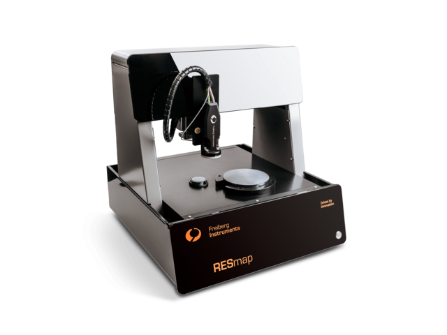
Skip breadcrumb navigation Breadcrumb Freiberg Instruments Products Resistivity Mapping RESmap RESmap High-Precision Resistivity Mapping System for Accurate Material Analysis Interested? Get in touch! Contact now Product Sheet Skip menu Quick navigation Features Applications Specifications Technology Software Contact Fast and reliable resistivity mapping tool for highly doped samples Exceptional Repeatability (sigma < 0.15%) Advanced Stability Sensors Seamless Inline Integration and Effortless Calibration Materials The RESmap is specialized on highly doped materials Si SiC and more Features & Benefits Sigma < 0.15 % exceptional repeatability Resistivity 1–100 mOhm cm Throughput > 20 Wafers/hour ± 5 % accuracy with temperature correction ± 5 % accuracy with temperature correction Exceptional Repeatability Achieves ultra-high precision with a standard deviation of less than 0.15%, ensuring consistent and reliable results. Advanced Stability Sensors Features an integrated distance and temperature sensor, maintaining superior measurement accuracy and stability Seamless Inline Integration Available as a fully automated, compact sensor, ideal for smooth and efficient inline applications Effortless Calibration Enables easy and stable calibration using a dedicated sample set, reducing setup time and ensuring long-term reliability Contact free measurement and imaging of the resistivity High frequency eddy current sensing principle with integrated IR temperature sensor to correct for temperature variations of the sample Material form factor Flat or slightly curved wafers, boules, ingots slabs, blanks and thin films X-Y placement resolution ≥ 0.1 mm Edge exclusion 5 mm Reliability modular, compact bench top instrument design for high reliability and uptime > 99% Measurement time < 3s for the measurement and < 1s between measurements Measurement speed < 30s for a 200 mm wafer/ingot, 9 points Bull´s eye chart management for maximum accuracy and precision Measurement principle of eddy current sensor Applications High precision Resistivity Measurement Measuring resistivity in highly doped semiconductors is crucial for several reasons:Quality control and Doping density verification, Device performance prediction, Extraction of material… Learn more RESmap delivers unmatched repeatability, stability and accuracy – making it the trusted choice for precise resistivity mapping across a wide range of materials. Dr. Christian Hagendorf Key Account Manager Interested? Our experts are happy to assist you. Get in touch! Contact us now! Prepared for Automation different platforms available Measurement method conforms with SEMI MF673 Data and data validity checked using NIST standards Accuracy over calibration interval ±1% Integrated IR temperature sensor (±0.1°) to allow reporting resistivity at a standard temperature, different from the actual temperature of the sample Sample thickness correction for samples where the penetration depth of the high frequency signal is larger than the penetration depth Power requirements 100-250 VAC, 5 A Dimensions (w/h/d) 465 x 550 x 600 mm Software control standard PC with Window 10 or latest, 2 Ethernet ports Download Product Flyer PDF (167 KB) Technologies Minority carrier lifetime The measured effective lifetime is composed of the bulk lifetime and surface lifetime, which depends on the surface properties of a sample. Hence the surface has to be passivated, if you want… Learn more Photoconductivity When light of sufficient energy is absorbed by a semiconductor, the number of free electrons and holes changes and raises the electrical conductivity of the semiconductor. This increase is… Learn more Resistivity The electrical resistivity directly depends on the density of the semiconductor and is therefore a useful parameter to monitor doping profiles and homogeneity. The lifetime and diffusion length… Learn more Mobility The mobility is a quantity related to the drift velocity of electrons or holes in an applied electric field across a material. The mobility depends on different scattering processes that can… Learn more Diffusion length Learn more Defect properties The properties of a defect and its impact on the material quality can be described by three main parameters:defect concentration NT, capture cross sections for electrons and holes σn, σp,… Learn more Lifetime simulations From the simulated time dependent carrier concentrations the photoconductivity can be calculated using the mobility model of DORKEL and LETURCQ [2] . The minority carrier lifetime can be… Learn more Simulation of carrier profiles The measurement of thick samples as bricks leads to new questions and problems. One of these questions is how the carrier profiles that develops in a sample effect the lifetime measurements. To… Learn more Microwave detected photoconductivity (MDP) The novel method MDP is well suited for both, defect investigation by e.g. injection dependent minority carrier lifetime measurements, as well as mapping of wafers or even bricks for inline… Learn more Comparison to µ-PCD and QSSPC Besides MDP the two most important contact less lifetime measuring methods are QSSPC (quasi steady state photoconductivity) and µ-PCD (microwave detected photoconductive decay). Currently one… Learn more MD-PICTS MD-PICTS is a modification of MDP, where temperature dependent measurements of the defect part of the transient are accomplished. This allows for a spatially resolved defect characterization.… Learn more Penetration depth of different laser wavelength in silicon The microwave detected photoconductivity measures the photoconductivity after the irradiation of the sample with light. Usually the light should have an energy that is higher than the bandgap,… Learn more Materials Electrical properties and defects of a large variety of semiconductor materials, devices and dielectric materials can be investigated contact less and destruction with our advanced method MDP.… Learn more User-friendly and advanced operating software with Resistivity measurement recipes Export/import functions and raw data access Multi-level user account management Overview over all performed measurements Mapping options (line, cross, star, full map, topography, user defined pattern) Package of analysis functions; statistics, variance analysis, temperature correction functions and library Remote accessibility; Internet based based system allows remote operation and technical support from anywhere in the world Get in touch Do not hesitate to contact us – we are available to assist you with any inquiries or requests. Use our inquiry tool or reach out via email: sales @ freiberginstruments.com

Product

MDpicts

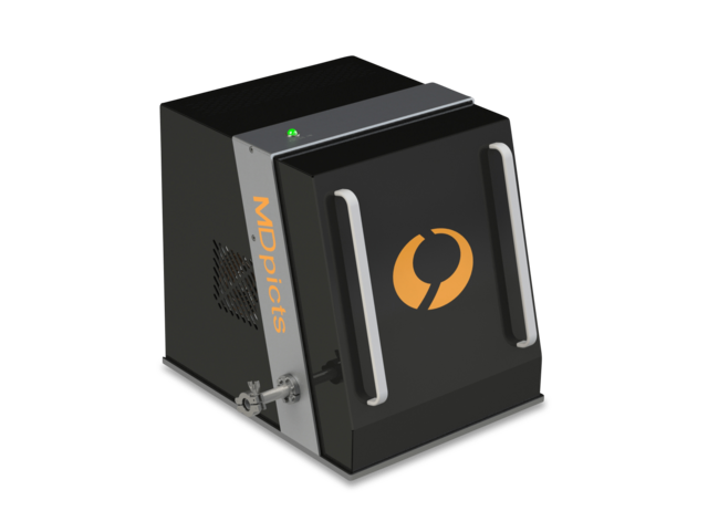
Skip breadcrumb navigation Breadcrumb Freiberg Instruments Products Microwave Detected Photoconductivity MDpicts MDpicts Temperature-Dependent Lifetime Measurement System for Advanced Material Analysis Interested? Get in touch! Contact now Product Sheet Laser Selection Guide Skip menu Quick navigation Features Applications Technology Contact Enables root cause analysis of material defects: destruction free, flexible and precise Cooling with stirling cooler without handling of liquid nitrogen Customized laser and optic integration for all your materials Fully automated temperature dependent measurements Materials The MDpicts enables the electrical characterization of almost all semiconductors Si SiC Ge GaAs Ga₂O₃ InP Diamond and more Features & Benefits 355–1550 nm Available wavelengths 10 ns Time resolution 30–300 K Temperature range Repetition < 60 min. Measurement time Repetition < 60 min. Measurement time Sensitivity: highest sensitivity for electrical defect characterization Temperature range: liquid nitrogen (77 K) up to 500 K. Optional: liquid helium (4 K) or higher temperatures Range of decay constants: 20 ns to several ms Contamination determination: measurement of fundamental trap level properties: activation energy and capture cross section of traps, temperature and injection dependent lifetime measurements Repeatability: > 99%, Measurement time: < 60 minutes. Liquid nitrogen consumption: 2 l/run Flexibility: select from different wavelengths from 365 nm up to 1480 nm for materials of different kinds Accessibility: IP based system allows remote operation and technical support from anywhere in the world From the slope of the Arrhenius plot (Fig. 3) the activation energy can be determined. With the novel commercially available MD-PICTS equipment it is possible to measure the temperature dependence of the photoconductivity transient in a range from 20…500 K. In the past Si, GaAs, InP, SiC and many more semiconductors have already been successfully investigated with this method. Download Product Sheet PDF (858 KB) Fig. 4: example of a MD-PICTS spectrum of different tempered Cz—Si wafers Fig. 1: Temperature dependent carrier emission transients Fig. 2: Box car evaluation with varying ID Fig. 3: Arrhenius plot In order to investigate defects in semiconductors it is widely spread to use temperature dependent methods as deep level transient spectroscopy (DLTS). Usually for these methods it is necessary to form contacts on the samples, which means the sample itself is often altered due to annealing steps. Furthermore for lot of semiconductors some effort is needed to create ohmic contacts at all. MD-PICTS is a non-destructive, contactless method with which the activation energies and capture cross sections of defects can be determined with a high accuracy. For MD-PICTS measurements the photoconductivity of a sample after the irradiation with light is measured with a resonant microwave cavity. For the determination of the activation energy the temperature dependent change of the photoconductivity transient is determined via a window analysis, which is also used for DLTS measurements (Fig. 1). Fig.2 shows a so called MD-PICTS spectrum which results from the window analysis. Every peak in this spectrum is a certain defect in the sample. The temperature shift of the maximum of this peak is plotted in an Arrhenius plot according to this formula of the emission rate: \(e_{n} = \gamma \sigma_{n}T^2e^{-\frac{E_{A}}{kT}}\) Applications Photoconductivity measurements and trap analysis Equipped with a 355 nm laser (μ-PCD) or a 375 nm laser diode (MDP), the MDPmap as well as the MDpicts from Freiberg Instruments are suitable for photoconductivity measurements and trap analysis… Learn more Microwave Detected Photo Induced Current Transient Spectroscopy In order to investigate defects in semiconductors it is widely spread to use temperature dependent methods as deep level transient spectroscopy (DLTS). Usually for these methods it is necessary… Learn more Minority carrier lifetime measurements on SiC In recent years the quality of SiC materials has improved profoundly and hence SiC is becoming more and more a competitor to Si for e.g. high-power devices. Since it is a wide-bandgap… Learn more Investigation of material quality of GaAs In contrast to other techniques MD-PICTS (microwave detected photo induced current transient spectroscopy) can detect signals even from thin surface regions (3 µm) of SI GaAs samples and is… Learn more Investigation of defect levels in InP MD-PICTS is a well suited method for the investigation of defect levels in InP. For example investigations on indium phosphide shows that the defect content changes during annealing processes,… Learn more Interested? Our experts are happy to assist you. Get in touch! Contact us now! Technologies Minority carrier lifetime The measured effective lifetime is composed of the bulk lifetime and surface lifetime, which depends on the surface properties of a sample. Hence the surface has to be passivated, if you want… Learn more Photoconductivity When light of sufficient energy is absorbed by a semiconductor, the number of free electrons and holes changes and raises the electrical conductivity of the semiconductor. This increase is… Learn more Resistivity The electrical resistivity directly depends on the density of the semiconductor and is therefore a useful parameter to monitor doping profiles and homogeneity. The lifetime and diffusion length… Learn more Mobility The mobility is a quantity related to the drift velocity of electrons or holes in an applied electric field across a material. The mobility depends on different scattering processes that can… Learn more Diffusion length Learn more Defect properties The properties of a defect and its impact on the material quality can be described by three main parameters:defect concentration NT, capture cross sections for electrons and holes σn, σp,… Learn more Lifetime simulations From the simulated time dependent carrier concentrations the photoconductivity can be calculated using the mobility model of DORKEL and LETURCQ [2] . The minority carrier lifetime can be… Learn more Simulation of carrier profiles The measurement of thick samples as bricks leads to new questions and problems. One of these questions is how the carrier profiles that develops in a sample effect the lifetime measurements. To… Learn more Microwave detected photoconductivity (MDP) The novel method MDP is well suited for both, defect investigation by e.g. injection dependent minority carrier lifetime measurements, as well as mapping of wafers or even bricks for inline… Learn more Comparison to µ-PCD and QSSPC Besides MDP the two most important contact less lifetime measuring methods are QSSPC (quasi steady state photoconductivity) and µ-PCD (microwave detected photoconductive decay). Currently one… Learn more MD-PICTS MD-PICTS is a modification of MDP, where temperature dependent measurements of the defect part of the transient are accomplished. This allows for a spatially resolved defect characterization.… Learn more Penetration depth of different laser wavelength in silicon The microwave detected photoconductivity measures the photoconductivity after the irradiation of the sample with light. Usually the light should have an energy that is higher than the bandgap,… Learn more Materials Electrical properties and defects of a large variety of semiconductor materials, devices and dielectric materials can be investigated contact less and destruction with our advanced method MDP.… Learn more For more information please read: [1] B. Berger, N. Schüler, S. Anger, B. Gruendig-Wendrock, J. R. Niklas, K. Dornich, physica status solidi A, 1-8 [2] C. R. Engst, I. Eisele, and C. Kutter, Defect characterization of unannealed neutron transmutation doped silicon by means of deep temperature microwave detected photo induced current transient spectroscopy, Journal of Applied Physics 127, 035704 (2020) [3] C. R. Engst, M. Rommel, C. Bscheid, I. Eisele and C. Kutter, Bulk lifetime characterization of corona charged silicon wafers with high resistivity by means of microwave detected photoconductivity, Journal of Applied Physics 122, 215704 (2017) Get in touch Do not hesitate to contact us – we are available to assist you with any inquiries or requests. Use our inquiry tool or reach out via email: sales @ freiberginstruments.com

Product

MDPlinescan

Skip breadcrumb navigation Breadcrumb Freiberg Instruments Products Microwave Detected Photoconductivity MDPlinescan MDPlinescan Versatile OEM Unit for Lifetime Measurements on Silicon Samples, from Bricks to Processed Wafers Interested? Get in touch! Contact now Product Sheet Laser Selection Guide Skip menu Quick navigation Features Applications Specifications Technology Contact Features & Benefits Inline line scanner or single spot measurement The MDPlinescan is an OEM unit designed for seamless integration into automated inspection systems. It performs carrier lifetime scans in real-time, typically with samples transported beneath the measurement head by a conveyor belt or robotic system. Applications span from silicon brick to wafer inspection, achieving measurement speeds of under one second per wafer. It is widely used for assessing incoming material quality in cell production lines and for process quality checks after passivation and diffusion, among other specialized applications. Integration is straightforward, requiring only an Ethernet connection and power supply. Facts allows for single wafer investigation recipe based measurements monitoring of material quality, process integrity and stability Advantages Measurement of minority carrier lifetime and resistivity lines cans at µ-PCD or steady state excitation conditions are in the focus of this small tool. OEM unit for the integration in production lines for multi- or monocrystalline silicon wafers at different preparation stages up to devices, bricks or ingots. Small size and standard automation interfaces allows for easy integration. Focus is put on long reliability and precision of measurement results. Applications Highly spatial resolved inline metrology on Multicrystalline Silicon Non-destructive measurements of minority carrier lifetime are well established and widely used for process control and characterization of defects in crystalline silicon. With our tool MDPinline… Learn more Determination of passivation homogeneity and surface recombination vel The measured or effective lifetime consists of the bulk lifetime and the surface lifetime, via: \(\cfrac{1}{\tau_{eff}} = \cfrac{1}{\tau_{bulk}} + \cfrac{1}{\tau_{surface}}\) That‘s why the… Learn more Interested? Our experts are happy to assist you. Get in touch! Contact us now! sample raw multi or mono wafers of multiple sizes like 156 mm², bricks, cells sample size above 50 x 50 mm² resistivity 0.2 - 10³ Ohm cm conduction type p, n material silicon wafers, partially or fully processed wafers, compound semiconductors and beyond measurable properties carrier lifetime hardware interface ethernet dimension 174 x 107 x 205 mm, weight: 3 kg power 24 V DC, 2 A Technologies Minority carrier lifetime The measured effective lifetime is composed of the bulk lifetime and surface lifetime, which depends on the surface properties of a sample. Hence the surface has to be passivated, if you want… Learn more Photoconductivity When light of sufficient energy is absorbed by a semiconductor, the number of free electrons and holes changes and raises the electrical conductivity of the semiconductor. This increase is… Learn more Resistivity The electrical resistivity directly depends on the density of the semiconductor and is therefore a useful parameter to monitor doping profiles and homogeneity. The lifetime and diffusion length… Learn more Mobility The mobility is a quantity related to the drift velocity of electrons or holes in an applied electric field across a material. The mobility depends on different scattering processes that can… Learn more Diffusion length Learn more Defect properties The properties of a defect and its impact on the material quality can be described by three main parameters:defect concentration NT, capture cross sections for electrons and holes σn, σp,… Learn more Lifetime simulations From the simulated time dependent carrier concentrations the photoconductivity can be calculated using the mobility model of DORKEL and LETURCQ [2] . The minority carrier lifetime can be… Learn more Simulation of carrier profiles The measurement of thick samples as bricks leads to new questions and problems. One of these questions is how the carrier profiles that develops in a sample effect the lifetime measurements. To… Learn more Microwave detected photoconductivity (MDP) The novel method MDP is well suited for both, defect investigation by e.g. injection dependent minority carrier lifetime measurements, as well as mapping of wafers or even bricks for inline… Learn more Comparison to µ-PCD and QSSPC Besides MDP the two most important contact less lifetime measuring methods are QSSPC (quasi steady state photoconductivity) and µ-PCD (microwave detected photoconductive decay). Currently one… Learn more MD-PICTS MD-PICTS is a modification of MDP, where temperature dependent measurements of the defect part of the transient are accomplished. This allows for a spatially resolved defect characterization.… Learn more Penetration depth of different laser wavelength in silicon The microwave detected photoconductivity measures the photoconductivity after the irradiation of the sample with light. Usually the light should have an energy that is higher than the bandgap,… Learn more Materials Electrical properties and defects of a large variety of semiconductor materials, devices and dielectric materials can be investigated contact less and destruction with our advanced method MDP.… Learn more Get in touch Do not hesitate to contact us – we are available to assist you with any inquiries or requests. Use our inquiry tool or reach out via email: sales @ freiberginstruments.com