Found 271 results in 2 milliseconds.

Product

MDpicts

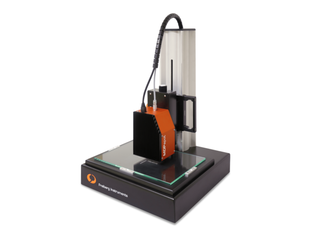
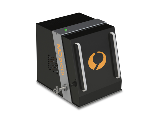
Skip breadcrumb navigation Breadcrumb Freiberg Instruments Products Microwave Detected Photoconductivity MDpicts MDpicts Temperature-Dependent Lifetime Measurement System for Advanced Material Analysis Interested? Get in touch! Contact now Product Sheet Laser Selection Guide Skip menu Quick navigation Features Applications Technology Contact Enables root cause analysis of material defects: destruction free, flexible and precise Cooling with stirling cooler without handling of liquid nitrogen Customized laser and optic integration for all your materials Fully automated temperature dependent measurements Materials The MDpicts enables the electrical characterization of almost all semiconductors Si SiC Ge GaAs Ga₂O₃ InP Diamond and more Features & Benefits 355–1550 nm Available wavelengths 10 ns Time resolution 30–300 K Temperature range Repetition < 60 min. Measurement time Repetition < 60 min. Measurement time Sensitivity: highest sensitivity for electrical defect characterization Temperature range: liquid nitrogen (77 K) up to 500 K. Optional: liquid helium (4 K) or higher temperatures Range of decay constants: 20 ns to several ms Contamination determination: measurement of fundamental trap level properties: activation energy and capture cross section of traps, temperature and injection dependent lifetime measurements Repeatability: > 99%, Measurement time: < 60 minutes. Liquid nitrogen consumption: 2 l/run Flexibility: select from different wavelengths from 365 nm up to 1480 nm for materials of different kinds Accessibility: IP based system allows remote operation and technical support from anywhere in the world From the slope of the Arrhenius plot (Fig. 3) the activation energy can be determined. With the novel commercially available MD-PICTS equipment it is possible to measure the temperature dependence of the photoconductivity transient in a range from 20…500 K. In the past Si, GaAs, InP, SiC and many more semiconductors have already been successfully investigated with this method. Download Product Sheet PDF (858 KB) Fig. 4: example of a MD-PICTS spectrum of different tempered Cz—Si wafers Fig. 1: Temperature dependent carrier emission transients Fig. 2: Box car evaluation with varying ID Fig. 3: Arrhenius plot In order to investigate defects in semiconductors it is widely spread to use temperature dependent methods as deep level transient spectroscopy (DLTS). Usually for these methods it is necessary to form contacts on the samples, which means the sample itself is often altered due to annealing steps. Furthermore for lot of semiconductors some effort is needed to create ohmic contacts at all. MD-PICTS is a non-destructive, contactless method with which the activation energies and capture cross sections of defects can be determined with a high accuracy. For MD-PICTS measurements the photoconductivity of a sample after the irradiation with light is measured with a resonant microwave cavity. For the determination of the activation energy the temperature dependent change of the photoconductivity transient is determined via a window analysis, which is also used for DLTS measurements (Fig. 1). Fig.2 shows a so called MD-PICTS spectrum which results from the window analysis. Every peak in this spectrum is a certain defect in the sample. The temperature shift of the maximum of this peak is plotted in an Arrhenius plot according to this formula of the emission rate: \(e_{n} = \gamma \sigma_{n}T^2e^{-\frac{E_{A}}{kT}}\) Applications Photoconductivity measurements and trap analysis Equipped with a 355 nm laser (μ-PCD) or a 375 nm laser diode (MDP), the MDPmap as well as the MDpicts from Freiberg Instruments are suitable for photoconductivity measurements and trap analysis… Learn more Microwave Detected Photo Induced Current Transient Spectroscopy In order to investigate defects in semiconductors it is widely spread to use temperature dependent methods as deep level transient spectroscopy (DLTS). Usually for these methods it is necessary… Learn more Minority carrier lifetime measurements on SiC In recent years the quality of SiC materials has improved profoundly and hence SiC is becoming more and more a competitor to Si for e.g. high-power devices. Since it is a wide-bandgap… Learn more Investigation of material quality of GaAs In contrast to other techniques MD-PICTS (microwave detected photo induced current transient spectroscopy) can detect signals even from thin surface regions (3 µm) of SI GaAs samples and is… Learn more Investigation of defect levels in InP MD-PICTS is a well suited method for the investigation of defect levels in InP. For example investigations on indium phosphide shows that the defect content changes during annealing processes,… Learn more Interested? Our experts are happy to assist you. Get in touch! Contact us now! Technologies Minority carrier lifetime The measured effective lifetime is composed of the bulk lifetime and surface lifetime, which depends on the surface properties of a sample. Hence the surface has to be passivated, if you want… Learn more Photoconductivity When light of sufficient energy is absorbed by a semiconductor, the number of free electrons and holes changes and raises the electrical conductivity of the semiconductor. This increase is… Learn more Resistivity The electrical resistivity directly depends on the density of the semiconductor and is therefore a useful parameter to monitor doping profiles and homogeneity. The lifetime and diffusion length… Learn more Mobility The mobility is a quantity related to the drift velocity of electrons or holes in an applied electric field across a material. The mobility depends on different scattering processes that can… Learn more Diffusion length Learn more Defect properties The properties of a defect and its impact on the material quality can be described by three main parameters:defect concentration NT, capture cross sections for electrons and holes σn, σp,… Learn more Lifetime simulations From the simulated time dependent carrier concentrations the photoconductivity can be calculated using the mobility model of DORKEL and LETURCQ [2] . The minority carrier lifetime can be… Learn more Simulation of carrier profiles The measurement of thick samples as bricks leads to new questions and problems. One of these questions is how the carrier profiles that develops in a sample effect the lifetime measurements. To… Learn more Microwave detected photoconductivity (MDP) The novel method MDP is well suited for both, defect investigation by e.g. injection dependent minority carrier lifetime measurements, as well as mapping of wafers or even bricks for inline… Learn more Comparison to µ-PCD and QSSPC Besides MDP the two most important contact less lifetime measuring methods are QSSPC (quasi steady state photoconductivity) and µ-PCD (microwave detected photoconductive decay). Currently one… Learn more MD-PICTS MD-PICTS is a modification of MDP, where temperature dependent measurements of the defect part of the transient are accomplished. This allows for a spatially resolved defect characterization.… Learn more Penetration depth of different laser wavelength in silicon The microwave detected photoconductivity measures the photoconductivity after the irradiation of the sample with light. Usually the light should have an energy that is higher than the bandgap,… Learn more Materials Electrical properties and defects of a large variety of semiconductor materials, devices and dielectric materials can be investigated contact less and destruction with our advanced method MDP.… Learn more For more information please read: [1] B. Berger, N. Schüler, S. Anger, B. Gruendig-Wendrock, J. R. Niklas, K. Dornich, physica status solidi A, 1-8 [2] C. R. Engst, I. Eisele, and C. Kutter, Defect characterization of unannealed neutron transmutation doped silicon by means of deep temperature microwave detected photo induced current transient spectroscopy, Journal of Applied Physics 127, 035704 (2020) [3] C. R. Engst, M. Rommel, C. Bscheid, I. Eisele and C. Kutter, Bulk lifetime characterization of corona charged silicon wafers with high resistivity by means of microwave detected photoconductivity, Journal of Applied Physics 122, 215704 (2017) Get in touch Do not hesitate to contact us – we are available to assist you with any inquiries or requests. Use our inquiry tool or reach out via email: sales @ freiberginstruments.com

Product

MDPpro 850+

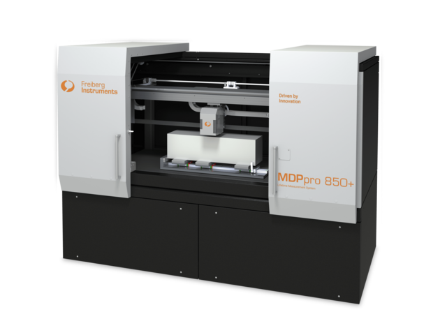
Skip breadcrumb navigation Breadcrumb Freiberg Instruments Products Microwave Detected Photoconductivity MDPpro 850+ MDPpro 850+ Advanced Solution for Quality Control of Monocrystalline Silicon Ingots, Bricks, and Wafers Interested? Get in touch! Contact now Product Sheet Skip menu Quick navigation Features Applications Specifications Technology Options Software Contact Materials For HJT, HIT, TOPcon, bifacial PERC, PERC+ solar cells and more. Si Perovskite and more Features & Benefits Range of lifetimes: 20 ns to 100 ms (for samples > 0.3 Ohm cm) SEMI standard: PV9-1110 Measurement speed: < 30 sec for linescan < 5 min for complete mapping Simultaneous measurement of: lifetime μPCD/MDP (QSS) and resistivity Automatic geometric recognition: G12, M10 bricks and wafers Slip lines in Cz-Si ingot Lifetime measurement of a quasi-mono Si ingot with a lot defects Applications Resistance measurements on wafers and bricks With MDPmap and MDPingot it is possible to measure the resistivity of wafers or bricks with a high accuracy and a resolution of 1 mm via eddy current measurements. The Eddy current sensor setup… Learn more Light Beam Induced Current (LBIC) The proceeding is based on the measurement of the local short circuit current Isc in the cell, which is produced through appropriate excitation. For the measurement the solar cell is contacted… Learn more Iron concentration determination With the MDPingot and MDPmap series it is possible to measure the iron concentration in bricks and wafers fully automated and with a very high resolution. Lifetime measurements before and after… Learn more p/n detection in bricks In the PV industry sometimes also low quality material with a high phosphorous concentration is used. Phosphor has a segregation coefficient of 0.35 and is therefore segregating in the top of the… Learn more Detection of CrB in silicon Lifetime measurements before and after chromium boron pair dissociation is a widely used method for chromium determination in silicon wafers. In boron doped silicon with a high doping… Learn more Detection of BO2 in silicon The boron-oxygen complexes can be activated by irradiating the sample with light and deactivated by heating the sample at 200 °C for several minutes. This can be used similar to the iron… Learn more Trap concentration determination With the MDPmap and MDPingot it is possible to measure the photoconductivity as well as the minority carrier lifetime with one measurement and fully automated in a wide injection range. A clever… Learn more Injection dependent measurements With MDPmap it is possible to measure not only injection dependent lifetime curves but also photoconductivity curves over a very wide range of injection. In the MDPmap and MDPingot up to 4… Learn more Inline metrology of mc-Si bricks With the MDPinline ingot it is possible to measure all 4 sides of a brick in under 1 min per side with 1 mm resolution. At the same time a spatial resolved measurement of conduction type changes… Learn more Photoconductivity measurements of implanted samples In this case not the lifetime, but the photoconductivity or signal height is the most sensitive parameter for detecting inhomogeneity in implantations. It depends strongly on the resistivity and… Learn more Lifetime determination of epitaxial silicon thin-film layers With MDP it is possible to measure the lifetime of minority carriers and the photoconductivity in epitaxial layers as fast and exactly as possible with a high resolution. The measurement of… Learn more Interested? Our experts are happy to assist you. Get in touch! Contact us now! Technical specifications Material monocrystalline silicon Ingot size between 125 x 125 to 210 x 210 mm², brick length 850 mm or longer Wafer Size up to 300 ¬mm diameter Resistivity range 0.5 – 5 Ohm cm. Other ranges on request Conduction type p, n Measurable properties lifetime - μPCD/MDP (QSS), photoconductivity, resistivity and more Default excitation lR laser diode (980 nm, max. 500 mW) and IR laser diode (905 nm, max. 9000 mW). Other wavelengths are available on request PC workstation Windows 11 or latest, .NET Framework update, 2 Ethernet ports Power requirements 100 – 250 V AC, 6 A Dimensions (W × H × D) 2560 × 1910 × 1440 mm Weight approx. 200 kg Certification manufactured under ISO 9001 guidelines, CE conform Download Product Sheet PDF (361 KB) Technologies Minority carrier lifetime The measured effective lifetime is composed of the bulk lifetime and surface lifetime, which depends on the surface properties of a sample. Hence the surface has to be passivated, if you want… Learn more Photoconductivity When light of sufficient energy is absorbed by a semiconductor, the number of free electrons and holes changes and raises the electrical conductivity of the semiconductor. This increase is… Learn more Resistivity The electrical resistivity directly depends on the density of the semiconductor and is therefore a useful parameter to monitor doping profiles and homogeneity. The lifetime and diffusion length… Learn more Mobility The mobility is a quantity related to the drift velocity of electrons or holes in an applied electric field across a material. The mobility depends on different scattering processes that can… Learn more Diffusion length Learn more Defect properties The properties of a defect and its impact on the material quality can be described by three main parameters:defect concentration NT, capture cross sections for electrons and holes σn, σp,… Learn more Lifetime simulations From the simulated time dependent carrier concentrations the photoconductivity can be calculated using the mobility model of DORKEL and LETURCQ [2] . The minority carrier lifetime can be… Learn more Simulation of carrier profiles The measurement of thick samples as bricks leads to new questions and problems. One of these questions is how the carrier profiles that develops in a sample effect the lifetime measurements. To… Learn more Microwave detected photoconductivity (MDP) The novel method MDP is well suited for both, defect investigation by e.g. injection dependent minority carrier lifetime measurements, as well as mapping of wafers or even bricks for inline… Learn more Comparison to µ-PCD and QSSPC Besides MDP the two most important contact less lifetime measuring methods are QSSPC (quasi steady state photoconductivity) and µ-PCD (microwave detected photoconductive decay). Currently one… Learn more MD-PICTS MD-PICTS is a modification of MDP, where temperature dependent measurements of the defect part of the transient are accomplished. This allows for a spatially resolved defect characterization.… Learn more Penetration depth of different laser wavelength in silicon The microwave detected photoconductivity measures the photoconductivity after the irradiation of the sample with light. Usually the light should have an energy that is higher than the bandgap,… Learn more Materials Electrical properties and defects of a large variety of semiconductor materials, devices and dielectric materials can be investigated contact less and destruction with our advanced method MDP.… Learn more Accessories & Options Our devices offer versatile configuration options to meet specific requirements effectively. Each model can be customized to ensure maximum flexibility and efficiency. Contact for more information Spot size variation Resistivity measurement (bricks/wafers) Background/Bias light Refl ection measurement (MDP) LBIC Internal iron mapping of p-doped Si P/N detection Bar code reader Automatic geometric recognition Wide range of lasers Software XRDStudio Multiple Operating ModesOperator Mode: Designed for fixed measurement parameters, ensuring a safe and streamlined workflow. Administrator Mode: Allows for the creation and modification of… Learn more Get in touch Do not hesitate to contact us – we are available to assist you with any inquiries or requests. Use our inquiry tool or reach out via email: sales @ freiberginstruments.com

Product

MDPspot

Skip breadcrumb navigation Breadcrumb Freiberg Instruments Products Microwave Detected Photoconductivity MDPspot MDPspot Quick and Simple Lifetime Measurement Made Easy Interested? Get in touch! Contact now Product Sheet Laser Selection Guide Skip menu Quick navigation Features Applications Specifications Technology Options Contact Enables fast and easy assessment of the lifetime at a single point Single point measurement Wafers and ingots Flexible low cost tool Materials Discover unparalleled ease and speed in lifetime characterization of almost all semiconductors with MDPspot, designed to streamline your workflow without compromising accuracy. Si SiC Ge GaN GaAs InP and more Features & Benefits 355–1550 nm Available wavelengths 10 ns Time resolution > 99 % repeatability Flexible measurement For wafers and ingots Flexible measurement For wafers and ingots contactless destruction free electrical semiconductor characterisation μ-PCD measurement option included advanced sensitivity for visualisation of so far invisible defects and investigations of epitaxial layers integration of up to four lasers for a wide range of injection levels access to primary data of single transients as well as maps for special evaluation purposes allows for single wafer investigation different recipes for different wafer classes monitoring of material, process quality and stability Table top single spot measurements The MDPspot is an affordable and compact solution for lifetime characterization of various semiconductors across different preparation stages. Designed without built-in automation, it offers flexibility for diverse applications. Cost-Effective Design : A budget-friendly option for reliable lifetime measurements. Versatile Compatibility : Suitable for a range of semiconductors samples, from thin wafers to thicker materials up to 156 mm bricks. Optional Z-Axis Adjustment : A hand-operated z-axis is available for precise handling of thicker samples. Intuitive Software : Standard software included for clear visualization and analysis of results. Streamline your measurement processes with this efficient and easy-to-use system. Applications Resistance measurements on wafers and bricks With MDPmap and MDPingot it is possible to measure the resistivity of wafers or bricks with a high accuracy and a resolution of 1 mm via eddy current measurements. The Eddy current sensor setup… Learn more Minority carrier lifetime measurements on SiC In recent years the quality of SiC materials has improved profoundly and hence SiC is becoming more and more a competitor to Si for e.g. high-power devices. Since it is a wide-bandgap… Learn more Investigation of material quality of GaAs In contrast to other techniques MD-PICTS (microwave detected photo induced current transient spectroscopy) can detect signals even from thin surface regions (3 µm) of SI GaAs samples and is… Learn more Injection dependent measurements With MDPmap it is possible to measure not only injection dependent lifetime curves but also photoconductivity curves over a very wide range of injection. In the MDPmap and MDPingot up to 4… Learn more Highly spatial resolved inline metrology on Multicrystalline Silicon Non-destructive measurements of minority carrier lifetime are well established and widely used for process control and characterization of defects in crystalline silicon. With our tool MDPinline… Learn more Determination of passivation homogeneity and surface recombination vel The measured or effective lifetime consists of the bulk lifetime and the surface lifetime, via: \(\cfrac{1}{\tau_{eff}} = \cfrac{1}{\tau_{bulk}} + \cfrac{1}{\tau_{surface}}\) That‘s why the… Learn more Interested? Our experts are happy to assist you. Get in touch! Contact us now! Technical specifications mono or multi silicon wafers, bricks, cells, wafers after ­different processing steps like passivation or diffusion sample size above 50 x 50 mm² up to 12“ or 210 x 210 mm² resistivity 0.2 - 10³ Ohm cm material silicon wafers, bricks, partially or fully processed wafers, compound semiconductors and beyond measureable properties carrier lifetime dimension 360 x 360 x 520 mm, weight: 16 kg power 110/220 V, 50/60 Hz, 3 A Technologies Minority carrier lifetime The measured effective lifetime is composed of the bulk lifetime and surface lifetime, which depends on the surface properties of a sample. Hence the surface has to be passivated, if you want… Learn more Photoconductivity When light of sufficient energy is absorbed by a semiconductor, the number of free electrons and holes changes and raises the electrical conductivity of the semiconductor. This increase is… Learn more Resistivity The electrical resistivity directly depends on the density of the semiconductor and is therefore a useful parameter to monitor doping profiles and homogeneity. The lifetime and diffusion length… Learn more Mobility The mobility is a quantity related to the drift velocity of electrons or holes in an applied electric field across a material. The mobility depends on different scattering processes that can… Learn more Diffusion length Learn more Defect properties The properties of a defect and its impact on the material quality can be described by three main parameters:defect concentration NT, capture cross sections for electrons and holes σn, σp,… Learn more Lifetime simulations From the simulated time dependent carrier concentrations the photoconductivity can be calculated using the mobility model of DORKEL and LETURCQ [2] . The minority carrier lifetime can be… Learn more Simulation of carrier profiles The measurement of thick samples as bricks leads to new questions and problems. One of these questions is how the carrier profiles that develops in a sample effect the lifetime measurements. To… Learn more Microwave detected photoconductivity (MDP) The novel method MDP is well suited for both, defect investigation by e.g. injection dependent minority carrier lifetime measurements, as well as mapping of wafers or even bricks for inline… Learn more Comparison to µ-PCD and QSSPC Besides MDP the two most important contact less lifetime measuring methods are QSSPC (quasi steady state photoconductivity) and µ-PCD (microwave detected photoconductive decay). Currently one… Learn more MD-PICTS MD-PICTS is a modification of MDP, where temperature dependent measurements of the defect part of the transient are accomplished. This allows for a spatially resolved defect characterization.… Learn more Penetration depth of different laser wavelength in silicon The microwave detected photoconductivity measures the photoconductivity after the irradiation of the sample with light. Usually the light should have an energy that is higher than the bandgap,… Learn more Materials Electrical properties and defects of a large variety of semiconductor materials, devices and dielectric materials can be investigated contact less and destruction with our advanced method MDP.… Learn more Accessories & Options Our devices offer versatile configuration options to meet specific requirements effectively. Each model can be customized to ensure maximum flexibility and efficiency. Contact for more information Spot size variation Resistivity measurement (wafers) Background/Bias light Reflection measurement (MDP) Software extension Additional lasers Get in touch Do not hesitate to contact us – we are available to assist you with any inquiries or requests. Use our inquiry tool or reach out via email: sales @ freiberginstruments.com

Product

MDPpro

Skip breadcrumb navigation Breadcrumb Freiberg Instruments Products Microwave Detected Photoconductivity MDPpro MDPpro Advanced Lifetime Measurement System for Quality Control and Material R&D on Semiconductors Interested? Get in touch! Contact now Product Sheet Laser Selection Guide Skip menu Quick navigation Features Applications Options Contact Materials Sophisticated Material Research & DevelopmentFew examples for research applications, Iron concentration determination Trap concentration determination Boron oxygen determination Injection dependent measurements and more Si SiC compound semiconductor Ge GaAs CdTe InP ZnS Perovskite oxides wide bandgap materials epitaxial layers and more Features & Benefits Throughput >240 bricks/day Speed > 99% Repeatability 1 mm cutting criteria for 156x156x400 m brick quality monitoring quality monitoring Contactless and destruction free lifetime imaging (μPCD/MDP (QSS)), photoconductivity, resistivity and p/n check according to semi standard SEMI PV9-1110 Wafer cutting, Furnace monitoring, Material optimization and more Best throughput: >240 bricks/day or >720 wafers/day Measurement speed: <4 minutes for a 156 x 156 x 400 mm standard brick Yield improvement : 1 mm cutting criteria for a 156 x 156 x 400 mm standard brick Quality control: designed for quality monitoring of processes and materials like mono or multi-crystalline silicon Contamination determination: metal (Fe) contaminations originated in crucibles and equipment Reliability: modular and rugged industrial instrument for higher reliability and uptime > 99% Repeatability: > 99% Resistivity: resistivity mapping without frequent calibration Facts completely contactless destruction free electrical semiconductor characterisation special “underneath the surface” lifetime measurement technique advanced sensitivity for visualisation of so far invisible defects automated cut criteria definition spacial resolved p/n conduction type transformation detection Applications Resistance measurements on wafers and bricks With MDPmap and MDPingot it is possible to measure the resistivity of wafers or bricks with a high accuracy and a resolution of 1 mm via eddy current measurements. The Eddy current sensor setup… Learn more Light Beam Induced Current (LBIC) The proceeding is based on the measurement of the local short circuit current Isc in the cell, which is produced through appropriate excitation. For the measurement the solar cell is contacted… Learn more Minority carrier Lifetime maps on 450 mm wafers Since several years, the microelectronic industry is planning to enlarge the wafer size from 300 mm (12 inch) to 450 mm (18 inch) diameter, in order to gain more yield. The technology for the… Learn more Iron concentration determination With the MDPingot and MDPmap series it is possible to measure the iron concentration in bricks and wafers fully automated and with a very high resolution. Lifetime measurements before and after… Learn more p/n detection in bricks In the PV industry sometimes also low quality material with a high phosphorous concentration is used. Phosphor has a segregation coefficient of 0.35 and is therefore segregating in the top of the… Learn more Detection of CrB in silicon Lifetime measurements before and after chromium boron pair dissociation is a widely used method for chromium determination in silicon wafers. In boron doped silicon with a high doping… Learn more Detection of BO2 in silicon The boron-oxygen complexes can be activated by irradiating the sample with light and deactivated by heating the sample at 200 °C for several minutes. This can be used similar to the iron… Learn more Trap concentration determination With the MDPmap and MDPingot it is possible to measure the photoconductivity as well as the minority carrier lifetime with one measurement and fully automated in a wide injection range. A clever… Learn more Injection dependent measurements With MDPmap it is possible to measure not only injection dependent lifetime curves but also photoconductivity curves over a very wide range of injection. In the MDPmap and MDPingot up to 4… Learn more Inline metrology of mc-Si bricks With the MDPinline ingot it is possible to measure all 4 sides of a brick in under 1 min per side with 1 mm resolution. At the same time a spatial resolved measurement of conduction type changes… Learn more Highly spatial resolved inline metrology on Multicrystalline Silicon Non-destructive measurements of minority carrier lifetime are well established and widely used for process control and characterization of defects in crystalline silicon. With our tool MDPinline… Learn more Determination of passivation homogeneity and surface recombination vel The measured or effective lifetime consists of the bulk lifetime and the surface lifetime, via: \(\cfrac{1}{\tau_{eff}} = \cfrac{1}{\tau_{bulk}} + \cfrac{1}{\tau_{surface}}\) That‘s why the… Learn more Photoconductivity measurements of implanted samples In this case not the lifetime, but the photoconductivity or signal height is the most sensitive parameter for detecting inhomogeneity in implantations. It depends strongly on the resistivity and… Learn more Lifetime determination of epitaxial silicon thin-film layers With MDP it is possible to measure the lifetime of minority carriers and the photoconductivity in epitaxial layers as fast and exactly as possible with a high resolution. The measurement of… Learn more Interested? Our experts are happy to assist you. Get in touch! Contact us now! Accessories & Options Spot size variation Resistivity measurement (bricks/wafers) Background/Bias light Reflection measurement (MDP) LBIC BiasMDP LBIC for solar cells LBIC, BiasMDP measurement stage with contacts Reference wafer Resistivity calibration set (bricks/wafers) Internal iron mapping of Si P/N detection Bar code reader Wide range of lasers Get in touch Do not hesitate to contact us – we are available to assist you with any inquiries or requests. Use our inquiry tool or reach out via email: sales @ freiberginstruments.com

Product

MDPlinescan

Skip breadcrumb navigation Breadcrumb Freiberg Instruments Products Microwave Detected Photoconductivity MDPlinescan MDPlinescan Versatile OEM Unit for Lifetime Measurements on Silicon Samples, from Bricks to Processed Wafers Interested? Get in touch! Contact now Product Sheet Laser Selection Guide Skip menu Quick navigation Features Applications Specifications Technology Contact Features & Benefits Inline line scanner or single spot measurement The MDPlinescan is an OEM unit designed for seamless integration into automated inspection systems. It performs carrier lifetime scans in real-time, typically with samples transported beneath the measurement head by a conveyor belt or robotic system. Applications span from silicon brick to wafer inspection, achieving measurement speeds of under one second per wafer. It is widely used for assessing incoming material quality in cell production lines and for process quality checks after passivation and diffusion, among other specialized applications. Integration is straightforward, requiring only an Ethernet connection and power supply. Facts allows for single wafer investigation recipe based measurements monitoring of material quality, process integrity and stability Advantages Measurement of minority carrier lifetime and resistivity lines cans at µ-PCD or steady state excitation conditions are in the focus of this small tool. OEM unit for the integration in production lines for multi- or monocrystalline silicon wafers at different preparation stages up to devices, bricks or ingots. Small size and standard automation interfaces allows for easy integration. Focus is put on long reliability and precision of measurement results. Applications Highly spatial resolved inline metrology on Multicrystalline Silicon Non-destructive measurements of minority carrier lifetime are well established and widely used for process control and characterization of defects in crystalline silicon. With our tool MDPinline… Learn more Determination of passivation homogeneity and surface recombination vel The measured or effective lifetime consists of the bulk lifetime and the surface lifetime, via: \(\cfrac{1}{\tau_{eff}} = \cfrac{1}{\tau_{bulk}} + \cfrac{1}{\tau_{surface}}\) That‘s why the… Learn more Interested? Our experts are happy to assist you. Get in touch! Contact us now! sample raw multi or mono wafers of multiple sizes like 156 mm², bricks, cells sample size above 50 x 50 mm² resistivity 0.2 - 10³ Ohm cm conduction type p, n material silicon wafers, partially or fully processed wafers, compound semiconductors and beyond measurable properties carrier lifetime hardware interface ethernet dimension 174 x 107 x 205 mm, weight: 3 kg power 24 V DC, 2 A Technologies Minority carrier lifetime The measured effective lifetime is composed of the bulk lifetime and surface lifetime, which depends on the surface properties of a sample. Hence the surface has to be passivated, if you want… Learn more Photoconductivity When light of sufficient energy is absorbed by a semiconductor, the number of free electrons and holes changes and raises the electrical conductivity of the semiconductor. This increase is… Learn more Resistivity The electrical resistivity directly depends on the density of the semiconductor and is therefore a useful parameter to monitor doping profiles and homogeneity. The lifetime and diffusion length… Learn more Mobility The mobility is a quantity related to the drift velocity of electrons or holes in an applied electric field across a material. The mobility depends on different scattering processes that can… Learn more Diffusion length Learn more Defect properties The properties of a defect and its impact on the material quality can be described by three main parameters:defect concentration NT, capture cross sections for electrons and holes σn, σp,… Learn more Lifetime simulations From the simulated time dependent carrier concentrations the photoconductivity can be calculated using the mobility model of DORKEL and LETURCQ [2] . The minority carrier lifetime can be… Learn more Simulation of carrier profiles The measurement of thick samples as bricks leads to new questions and problems. One of these questions is how the carrier profiles that develops in a sample effect the lifetime measurements. To… Learn more Microwave detected photoconductivity (MDP) The novel method MDP is well suited for both, defect investigation by e.g. injection dependent minority carrier lifetime measurements, as well as mapping of wafers or even bricks for inline… Learn more Comparison to µ-PCD and QSSPC Besides MDP the two most important contact less lifetime measuring methods are QSSPC (quasi steady state photoconductivity) and µ-PCD (microwave detected photoconductive decay). Currently one… Learn more MD-PICTS MD-PICTS is a modification of MDP, where temperature dependent measurements of the defect part of the transient are accomplished. This allows for a spatially resolved defect characterization.… Learn more Penetration depth of different laser wavelength in silicon The microwave detected photoconductivity measures the photoconductivity after the irradiation of the sample with light. Usually the light should have an energy that is higher than the bandgap,… Learn more Materials Electrical properties and defects of a large variety of semiconductor materials, devices and dielectric materials can be investigated contact less and destruction with our advanced method MDP.… Learn more Get in touch Do not hesitate to contact us – we are available to assist you with any inquiries or requests. Use our inquiry tool or reach out via email: sales @ freiberginstruments.com

Product

MDpicts pro

Skip breadcrumb navigation Breadcrumb Freiberg Instruments Products Microwave Detected Photoconductivity MDpicts pro MDpicts pro High-Resolution, Temperature-Dependent Lifetime Measurement System for Precise Material Characterization Interested? Get in touch! Contact now Product Sheet Laser Selection Guide Skip menu Quick navigation Features Applications Specifications Technology Contact Enables root cause analysis of material defects: destruction free, flexible and precise High spatial resolution Customized laser and optic integration for all your materials Novel cryostat for samples up to 4’’ Materials The MDpicts pro enables the electrical characterization of almost all semiconductors Si SiC Ge GaAs Ga₂O₃ InP Diamond and more Features & Benefits 355–1550 nm Available wavelengths 10 ns Time resolution 83–300 K Temperature range 10 µm Spatial resolution 10 µm Spatial resolution Applications Light Beam Induced Current (LBIC) The proceeding is based on the measurement of the local short circuit current Isc in the cell, which is produced through appropriate excitation. For the measurement the solar cell is contacted… Learn more Microwave Detected Photo Induced Current Transient Spectroscopy In order to investigate defects in semiconductors it is widely spread to use temperature dependent methods as deep level transient spectroscopy (DLTS). Usually for these methods it is necessary… Learn more Investigation of defect levels in InP MD-PICTS is a well suited method for the investigation of defect levels in InP. For example investigations on indium phosphide shows that the defect content changes during annealing processes,… Learn more Interested? Our experts are happy to assist you. Get in touch! Contact us now! Technical specifications temperature range 83 – 350 K sample size up to 4" wafers small wafer pieces resistivity 0.2 - >10 10 Ωcm conduction type p,n minority carrier lifetime 20 ns – 100 ms measurable properties lifetime, photoconductivity, activation energy, etc. excitation 355 – 1550 nm Technologies Minority carrier lifetime The measured effective lifetime is composed of the bulk lifetime and surface lifetime, which depends on the surface properties of a sample. Hence the surface has to be passivated, if you want… Learn more Photoconductivity When light of sufficient energy is absorbed by a semiconductor, the number of free electrons and holes changes and raises the electrical conductivity of the semiconductor. This increase is… Learn more Resistivity The electrical resistivity directly depends on the density of the semiconductor and is therefore a useful parameter to monitor doping profiles and homogeneity. The lifetime and diffusion length… Learn more Mobility The mobility is a quantity related to the drift velocity of electrons or holes in an applied electric field across a material. The mobility depends on different scattering processes that can… Learn more Diffusion length Learn more Defect properties The properties of a defect and its impact on the material quality can be described by three main parameters:defect concentration NT, capture cross sections for electrons and holes σn, σp,… Learn more Lifetime simulations From the simulated time dependent carrier concentrations the photoconductivity can be calculated using the mobility model of DORKEL and LETURCQ [2] . The minority carrier lifetime can be… Learn more Simulation of carrier profiles The measurement of thick samples as bricks leads to new questions and problems. One of these questions is how the carrier profiles that develops in a sample effect the lifetime measurements. To… Learn more Microwave detected photoconductivity (MDP) The novel method MDP is well suited for both, defect investigation by e.g. injection dependent minority carrier lifetime measurements, as well as mapping of wafers or even bricks for inline… Learn more Comparison to µ-PCD and QSSPC Besides MDP the two most important contact less lifetime measuring methods are QSSPC (quasi steady state photoconductivity) and µ-PCD (microwave detected photoconductive decay). Currently one… Learn more MD-PICTS MD-PICTS is a modification of MDP, where temperature dependent measurements of the defect part of the transient are accomplished. This allows for a spatially resolved defect characterization.… Learn more Penetration depth of different laser wavelength in silicon The microwave detected photoconductivity measures the photoconductivity after the irradiation of the sample with light. Usually the light should have an energy that is higher than the bandgap,… Learn more Materials Electrical properties and defects of a large variety of semiconductor materials, devices and dielectric materials can be investigated contact less and destruction with our advanced method MDP.… Learn more Get in touch Do not hesitate to contact us – we are available to assist you with any inquiries or requests. Use our inquiry tool or reach out via email: sales @ freiberginstruments.com

Product

HTpicts

Skip breadcrumb navigation Breadcrumb Freiberg Instruments Products Microwave Detected Photoconductivity HTpicts HTpicts Advanced High-Temperature Lifetime Measurement System for In-Depth Material Analysis Interested? Get in touch! Contact now Laser Selection Guide Skip menu Quick navigation Features Applications Contact Enables root cause analysis of deep material defects: destruction free, flexible and precise High temperatures for investigation of deep defect Customized laser and optic integration for all your materials Fully automated temperature dependent measurements Materials The HTpicts is specialized on deep defects in wide bandgap semiconductors SiC GaN AIN Ga₂O₃ Diamond and more Features & Benefits 355–1550 nm Available wavelengths 10 ns Time resolution 300–800 K Temperature range Extensive analysis Large software package Extensive analysis Large software package Applications Microwave Detected Photo Induced Current Transient Spectroscopy In order to investigate defects in semiconductors it is widely spread to use temperature dependent methods as deep level transient spectroscopy (DLTS). Usually for these methods it is necessary… Learn more Investigation of defect levels in InP MD-PICTS is a well suited method for the investigation of defect levels in InP. For example investigations on indium phosphide shows that the defect content changes during annealing processes,… Learn more Get in touch Do not hesitate to contact us – we are available to assist you with any inquiries or requests. Use our inquiry tool or reach out via email: sales @ freiberginstruments.com

Product

GM 2100

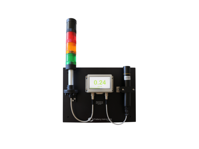
Skip breadcrumb navigation Breadcrumb Freiberg Instruments Products Radiation Monitoring Systems GM 2100 GM 2100 Gamma Radiation Monitor Interested? Get in touch! Contact now Skip menu Quick navigation Features Contact Features & Benefits Compact design Wall mounted Audio and visual alarms Plug and play Detector low range gamma radiation detector internal calibration factor splash proof aluminium housing measuring range: 0.1 μSv/h to 10 mSv/h accuracy: ±10% reading within the measuring range Electronics 4“ TFT touchscreen with a resolution of 480 x 272 pixels adjustable alarm limits local signalization of alarms via. light tower with buzzer potential-free relay contacts for external signalization Get in touch Do not hesitate to contact us – we are available to assist you with any inquiries or requests. Use our inquiry tool or reach out via email: sales @ freiberginstruments.com

Page

Publications

Publications for Luminescence and ESR dating Material Research Cimmino, A., Olšovcová, V., Versaci, R., Horváth, D., Lefebvre, B., Tsinganis, A., Trunečková, Z. Radiation Protection at Petawatt Laser-Driven Accelerator Facilities: The ELI Beamlines Case. Nuclear Science and Engineering, 198(2), 245–263. doi.org/10.1080/00295639.2023.2191585 Luminescence detectors at a laser-based electron accelerator A. Cimmino, I. Ambrožová, Ž. Knežević c, M. Majer c, D. Horváth a, C.M. Lazzarini a d, G.M. Grittani a, R. Truneček a, V. Olšovcová a, doi.org/10.1016/j.radmeas.2024.107367 A Cimmino, D Horváth, V Olšovcová, V Stránský, R Truneček and R Versaci Characterization of OSL dosimeters used at the ELI-beamlines laser-driven accelerator facility, A Cimmino et al 2021 J. Radiol. Prot. 41 N23, iopscience.iop.org/article/10.1088/1361-6498/ac14d5 Anna Cimmino, Iva Ambrožová, Silvia Motta, Roberto Versaci, Veronika Olšovcová, David Chvátil, Václav Olšanský, Roman Truneček, Andriy Velyhan, Vojtěch Stránský, Jaroslav Šolc. COMPARISON OF OSL AND TL DOSEMETERS WITH DATA COLLECTED AT THE MT25 CYCLIC ELECTRON ACCELERATOR, Radiation Protection Dosimetry, Volume 198, Issue 9-11, August 2022, Pages 670–674, doi.org/10.1093/rpd/ncac117 L. Oster, I. Eliyahu, Y.S. Horowitz, G. Reshes, A. Shapiro and G. Garty Demonstration of the potential and difficulties of combined TL and OSL measurements of TLD-600 and TLD-700 for the determination of the dose components in complex nuetron-gamma radiation fields. Radiation protection dosimetry. 188. 10.1093/rpd/ncz297. I Eliyahu, Y S Horowitz, G Reshes, A Shapiro, S Biderman, Y Assor, D Ginsburg, B Herman and L Oster Study of thermally and optically stimulated luminescence in LiF:Mg,Ti following neutron and beta irradiation. Eliyahu et al 2022 J. Phys.: Conf. Ser. 2298 012007 M.W. Kielty, M. Dettmann, V. Herrig, M.G. Chapman, M.R. Marchewka, A.A. Trofimov, U. Akgun, and L.G. Jacobsohn Investigation of Ce3+ luminescence in borate-rich borosilicate glasses. Journal of Non-Crystalline Solids 471 (2017) 357-361 Z. Chen, A.A. Trofimov, L.G. Jacobsohn, H. Xiao, K. Kornev, D. Xu, and F. Peng Transport properties of YAG:Er 3+ fiber membrane scintillators prepared by novel sol-gel/electrospinning method A.A. Trofimov, C. Li, K.S. Brinkman, and L.G. Jacobsohn Luminescence investigation of Ce incorporation in garnet-type Li 7 La 3 Zr 2 O 12 J. Lei, A.A. Trofimov, J. Chen, Z. Chen, Y. Hong, L. Yuan, W. Zhu, Q. Zhang, L.G. Jacobsohn, F. Peng, R.K. Bordia, and H. Xiao Thick Er-doped silica films sintered using CO2 laser for scintillation applications Y. Hong, Z. Chen, A.A. Trofimov, J. Lei, J. Chen, L. Yuan, W. Zhu, H. Xiao, D. Xu, L.G. Jacobsohn, K.G. Kornev, R.K. Bordia, and F. Peng Direct inkjet printing of miniaturized luminescent YAG:Er 3+ from sol-gel precursor Portakal, Z. G., Dogan, T., Yegen, S. B., Küçük, N., Ayvacikli, M., Guinea, J. G., Canimoglu, A., Karabulut, Y., Topaksu, M., and Can N. Luminescence characteristics of Dy 3+ incorporated zinc borate powders G.D. Patra, S.G. Singh, B. Tiwari, A.K. Singh, D.G. Desai, M. Tyagi, S. Sen, S.C. Gadkari Optically stimulated luminescence in Ag doped Li 2 B 4 O 7 single crystal and its sensitivity to neutron detection and dosimetry in OSL mode Luminescence Dating and Dosimetry Davis H, Siebers JV, Wijesooriya K, Mistro M. Clinical validation ofmyOSLchip: A beryllium oxide opticallystimulated luminescent dosimeter (OSLD)system in radiotherapy dosimetry . J Appl ClinMed Phys. 2025;26:e70094. Alexandra Drakopoulou, Polymnia Glampedaki, Vasiliki Peppa, Efi Koutsouveli, Georgios Kollias, Pantelis Karaiskos, Eleftherios P. Pappas, Suitability of a BeO-based OSLD system for end-to-end remote dosimetry tests in SRS/SRT applications , Physica Medica, Volume 133, 2025, 104975, ISSN 1120-1797. Murari M, Kreutzer S, Frouin M, Friedrich J, Lauer T, Klasen N, Schmidt C, Tsukamoto S, Richter D, Mercier N, Fuchs M. Infrared Radiofluorescence (IR-RF) of K-Feldspar: An Interlaboratory Comparison. Geochronometria. 2021;48(1): 95-110. Barbara Mauz, Loïc Martin, Michael Discher, Chantal Tribolo, Sebastian Kreutzer, Chiara Bahl, Andreas Lang, and Nobert Mercier Technical note: On the reliability of laboratory beta-source calibration for luminescence dating Madhav Krishna Murari, Sebastian Kreutzer, Georgina King, Marine Frouin, Sumiko Tsukamoto Christoph Schmidt, Tobias Lauer, Nicole Klasen, Daniel Richter, Johannes Friedrich, Norbert Mercier, Markus Fuchs Infrared radiofliorescence (IR-RF) dating: A review M. Discher, K. Dornich, A. Richter, B. Mauz and A. Lang Extending the measurement temperature range in a fully automated luminescence reader to -50 °C D. Richter, C.Woda and K. Dornich A new quartz for γ-transfer calibration of radiation sources Céline Bassinet and Wendy Le Bris TL investigation of glasses from mobile phone screen protectors for radiation accident dosimetry Sontag-González, M., Frouin, M., Li, B., and Schwenninger, J.-L. Accesing the dating potential of violet stimulated luminescence protocols Detlev Degering, Albrecht Degering Change is the only constant - time-dependent dose rates in luminescence dating Tristan Carter, Daniel A. Contreras, Justin Holcomb, Danica D. Mihailović, Panagiotis Karkanas, Guillaume Guérin, Ninon Taffin, Dimitris Athanasoulis, Christelle Lahaye Earliest occupation of the Central Aegean (Naxos), Greece: Implications for hominin and Homo sapiens’ behavior and dispersals Crassard, R., Hilbert, Y. H., Preusser, F., Wulf, G., and Schiettecatte, J. (2018). Middle Palaeolithic occupations in central Saudi Arabia during MIS 5 and MIS 7: new insights on the origins of the peopling of Arabia. Archaeological and Anthropological Sciences, 10.1007/s12520-018-0743-2. S. Kreutzer, L. Martin, C. Tribolo, P. Selva and N. Mercier Environmental dose rate determination using a passive dosimeter: Techniques and Workflow for ∝-Al 2 O 3 :C Chips N. Gribenski, K. N. Jansson, F. Preusser, J. M. Harbor, A. P. Stroeven, M. Trauerstein, R. Blomdin, J. Heyman, M. W. Caffee, N. A. Lifton, W. Zhang Re-evaluation of MIS 3 glaciation using cosmogenic radionuclide and single grain luminescence ages, Kanas Valley, Chinese Altai C. Bassinet, S. Kreutzer, N. Mercier, I. Clairand Violet stimulated luminescence signal from electronic components for radiation accident dosimetry Janet Ayobami Ademola, Clemens Woda, Emanuela Bortolin Thermoluminescence investigations on tobacco dust as an emergency dosimeter A.C. Cunningham, L. Clark-Balzan Overcoming crosstalk in luminescence images of mineral grains Tanuj Shukla, Manish Mehta, Manoj K. Jaiswal, Pradeep Srivastava, D.P. Dobhal, H.C. Nainwal, Atul K. Singh Late Quaternary glaciation history of monsoon-dominated Dingad basin, central Himalaya, India Merle Murua, Alar Rosentaua, Frank Preusserb, Jüri Pladoa, Ivo Sibula, Argo Jõelehta, Stefan Bjursäterc, Raivo Aunapa, Aivar Kriiskad Reconstructing Holocene shore displacement and Stone Age palaeogeography from a foredune sequence on Ruhnu Island, Gulf of Riga, Baltic Sea Daniel Richter, Philip Klinger, Christoph Schmidt, Paul van den Bogaard, Ludwig Zöller New chronometric age estimates for the context of the Neanderthal from Wannen-Ochtendung (Germany) by TL and argon dating Frank Preusser, Jan-Hendrik May, David Eschbach, Mareike Trauerstein, Laurent Schmitt Infrared stimulated luminescence dating of 19th century fluvial deposits from the upper Rhine River Ceri Shipton, Alison Crowther, Nikos Kourampas, Mary E. Prendergast, Mark Horton, Katerina Douka, Jean-Luc Schwenninger, Patrick Faulkner, Eréndira M. Quintana Morales, Michelle C. Langley, Ruth Tibesasa, Llorenc Picornell-Gelabert, Edwin N. Wilmsen, Chris Doherty, Margaret Ashley Veall, Abdallah K. Ali, Michael D. Petraglia & Nicole Boivin Reinvestigation of Kuumbi Cave, Zanzibar, reveals Later Stone Age coastal habitation, early Holocene abandonment and Iron Age reoccupation Vilumaa K., Tõnisson H., Sugita S., Buynevich I.V., Kont A., Muru M., Preusser F., Bjursäter S., Vaasma T., Vandel E., Molodkov A., and Järvelill J.I., Past extreme events recorded in the internal architecture of coastal formations in the Baltic Sea Region Juliana de Araujo Bibiano, Helen Jamil Khoury, Álvaro Barbosa de Carvalho Júnior Study of the Luminescent Properties from Brazilian Natural Flourite D. Richter, D. Mittelstraß, S. Kreutzer, R. Pintaske, K. Dornich, M. Fuchs A new fully integrated X-ray irrdiator system for dosimetric research D. Richter, A. Richter, K. Dornich lexsyg smart - A luminescence detection system for Dosimtery, Material Research and Dating application D. Richter, P. Klinger, L. Zöller Palaeodose underestimation of heated quartz in Red-TL dating of volcanic contexts C. Schmidt, J. Friedrich, L. Zöller Thermochronometry using red TL of quartz? - Numerical simulation and observations from in situ drill-hole samples J. Lomax, D. Mittelstraß, S. Kreutzer, M. Fuchs OSL, TL and IRSL emission spectra of sedimentary quartz and feldspar samples S. Huot, M. Frouin, M. Lamothe Evidence of shallow TL peaks contributions in infrared radiofluorescence M. Hernandez, N. Mercier Characteristics of the post-blue VSL signal from sedimentary quartz N. Gribenski, F. Preusser, S. Greilich, S. Huot, D. Mittelstraß Investigation of cross talk in single grain luminescence measurements using an EMCCD camera M. Frouin, S. Huot, N. Mercier, C. Lahaye, M. Lamothe The issue of laboratory bleaching in the infrared-radiofluorescence dating method S. Greilich, N. Gribenski, D. Mittelstraß, K. Dornich, S. Huot, F. Preusser Single-grain dose-distribution measurements by optically stimulated luminescence using an integrated EMCCD-based system A. Richter, D. Richter, K. Dornich A variety of Optional Luminescence Stimulation sources for lexsyg devices S. Kreutzer, S. Grehl, M. Dietze, C. Burrow, M.C. Fuchs, M. Fischer, C. Schmidt Investigating cold light: The R package Luminescence - signal, statistics and dating of environmental dynamics D. Richter, A. Richter, K. Dornich lexsyg - a new system for luminescence research D. Richter, R. Pintaske, K. Dornich, M. Krbetschek A novel beta source design for uniform irradiation in dosimetric applications
Application

Defects in 4H-SiC

Defects in 4H-SiC Investigated by surface photovoltage spectroscopy Defects in 4H-SiC investigated by surface photovoltage spectroscopy – power semiconductors Silicon carbide (SiC) high power, high voltage semiconductor devices lead the way not only for superfast chargers and on-board chargers for electrical vehicles (EV), but also power drive trains and power converters for traction applications such as light rails, trams and subways. Traction applications, as well as industrial motor drives, require power semiconductor switches with blocking voltages of 1200 V, 1700 V, 3300 V or even 4500 V (6500 V is still being explored). Reliability, lifetime and safety of the high power, high voltage semiconductor devices are the key parameters to control at the moment, where the commercially available 150 mm SiC wafers still suffer from some fundamental quality issues related to defects in bandgap of the SiC semiconductor. These issues will still remain on 200 mm SiC wafers, and it is therefore of extreme importance to be able to measure and report the state of the defects before, during and after device fabrication. The SPVcheck tool equipped with 3 UV light sources with centre wavelengths 355 nm, 365 nm and 450/660 nm is the ideal platform for epitaxial SiC wafer characterization, because it can be used to check the fundamental bandgap edge in a very elegant and fast way. The 450 nm or 660 nm wavelength is used as a baseline reference measurement, because the energy is too low to excite carriers in the SiC material. The 355 nm and 365 nm UV light sources are applied at the same time to the epitaxial SiC wafer, thereby creating a broad square like pulse covering energies in 3.25 to 3.55 eV in one shot. The transient SPV is measured in the time range from 10 ns and up to 10 ms. If the epitaxial layer on the SiC wafer has too many defects, the excitation of carriers will be weakened and the change in signal over time will be smaller. A perfect epitaxial layer, on the other hand, will have a higher output signal and, more importantly, sharp energy transition peaks in the ms range. An additional advantage of the square like energy pulse is the fact that the absorption coefficient of SiC is growing linearly with the square of the energy and is heavily temperature dependent. Therefore, by adding a temperature stage, the penetration depth of the UV light can be varied over a large range. Obviously the 355 nm and the 365 nm light sources does not need to switched on at the same time – they can be switched on and off in a modulated pattern with up to 1 kHz switching frequency or very long on and off cycles. Perfect 4H-SiC; Such a sharp transition will generate a large time-resolved signal change, probably around 10-100 µs 4H-SiC with defects; no sharp transitions will result in a small time-resolved signal change, probably < 1 µs Related Solutions and Industries: Epitaxial Layers & Thin Films Matching Products SPS/SPV series HR-SPSmap with fixed energy excitation sources High-Resolution and Sensitive Surface Photovoltage Measurement Solutions Learn more SPS/SPV series HR-SPSmap with variable energy excitation source with a variable energy excitation source Learn more Get in touch Do not hesitate to contact us – we are available to assist you with any inquiries or requests. Use our inquiry tool or reach out via email: sales @ freiberginstruments.com