Found 271 results in 1 milliseconds.

Product

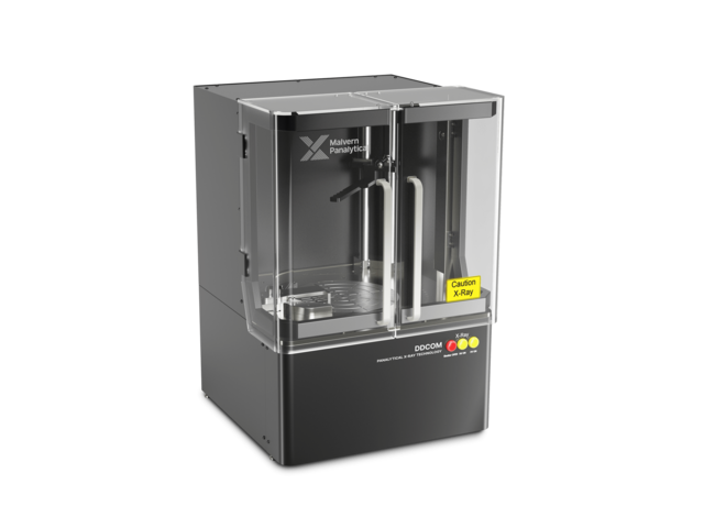
DDCOM

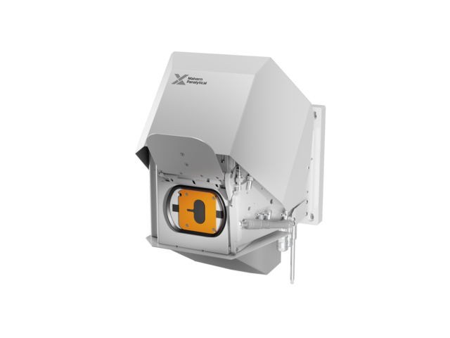
Skip breadcrumb navigation Breadcrumb Freiberg Instruments Products X-ray Diffraction DDCOM DDCOM Ultra-fast, bottom surface measuring crystal orientation in a compact package Exclusively through Malvern Panalytical Contact for demo Product Sheet Skip menu Quick navigation Features Applications Specifications Technology Options Software Contact Materials With DDCOM, a wide variety of materials can be precisely analyzed. Thanks to their flexibility and performance, our systems meet even the most demanding requirements. Ag Al₂O₃ (sapphire) AlSb Au CdTe GaAs GaN GaP GaPO₄ GaSb Ge InAs InP InSb La₃Ga₅SiO₁₄ LaTiO₃ LiF LiNbO₃ Mg₂SiO₄ MgAl₂O₄ MgF₂ MgO NdGaO₃ Ni PbS PbTe Pt Si SiC 2H SiC 4H SiC 6H SiC 15R SiC₃C SiO₂ (quartz) SnTe SrLaAlO₄ SrTiO₃ TiO₂ ZnO ZnTe and more Features & Benefits Ultra-fast Omega-scan approach 200 times faster than Theta-scan method Automatic evaluation of the complete lattice orientation in 3D Determination of entire crystal orientation within 5 seconds Efficient workflows for quality control For standard research and industrial workflows Azimuthal setting and marking of crystal orientation Preprogrammed cubic crystal parameters State-of-the-art and convenient software High precision, i.e up to (1/100)° Compact, user friendly and cost effective Easily movable and lightweight desktop design Convenient sample handling and easy to operate Low energy consumption and operating costs due to air cooled X-ray tube (no water cooling required) Control of cutting, grinding and lapping Complete lattice orientation of single crystals Suitable for a unique variety of materials in a large range of size and weight, such as: Wafers from 2-12” and Ingots up to 20kg Highlights Determination of the complete lattice orientation of single crystals Ultra-fast crystal orientation measurement using the Omega-scan method Determination of the arbitrary unknown orientation of cubic crystals Designed especially for azimuthal setting and marking of lattice directions Air cooled X-ray tube, no water cooling required Appropriate for research and production quality control Omega-scan diagram (Quartz) easy sample allignment Omega-scan method: All desired crystal orientation parameters are captured in one rotation within 5 seconds. Applications Samples with a wide variety of geometry & size The industrial synthesis of single crystals begins with large, heavy boules and is processed down to smaller forms, such as wafers or blanks. In experimental growth, tiny cylinders are produced.… Learn more Marking and measuring of in-plane directions The Omega Scan provides a complete crystal orientation in a single measurement, allowing for the direct identification of in-plane directions. This feature is particularly useful for marking… Learn more DDCOM – Exclusively through Malvern Panalytical This product is distributed by our trusted partner. Contact for demo Technical specifications X-ray source 30 W air-cooled X-ray tube, Cu anode Detectors Two scintillation counters Sample holder Precise turntable, setting accuracy 0.01°, tools for defined sample positioning and marking Dimensions 600 mm × 600 mm × 850 mm Weight 80 kg Power supply 100-230 V, 100 W, single phase Room temperature ≤ 30° C Technologies Omega-scan Ultra-Fast Orientation Measurement for Single Crystals Learn more Theta-scan Precision X-ray Method for Single Crystal Orientation Learn more Accessories & Options Device for mapping of wafers (maximum diameter 225 mm) Device for automatic loading from cassettes Software XRDStudio Multiple Operating ModesOperator Mode: Designed for fixed measurement parameters, ensuring a safe and streamlined workflow. Administrator Mode: Allows for the creation and modification of… Learn more DDCOM – Exclusively through Malvern Panalytical This product is distributed by our trusted partner. Contact for demo

Product

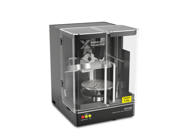
SDCOM

Skip breadcrumb navigation Breadcrumb Freiberg Instruments Products X-ray Diffraction SDCOM SDCOM Ultra-fast, top surface measuring crystal orientation in a compact package Exclusively through Malvern Panalytical Contact for demo Product Sheet Skip menu Quick navigation Features Applications Technology Software Contact Materials With SDCOM, a wide variety of materials can be precisely analyzed. Thanks to their flexibility and performance, our systems meet even the most demanding requirements. Ag Al₂O₃ (sapphire) AlSb Au CdTe GaAs GaN GaP GaPO₄ GaSb Ge InAs InP InSb La₃Ga₅SiO₁₄ LaTiO₃ LiF LiNbO₃ Mg₂SiO₄ MgAl₂O₄ MgF₂ MgO NdGaO₃ Ni PbS PbTe Pt Si SiC 2H SiC 4H SiC 6H SiC 15R SiC₃C SiO₂ (quartz) SnTe SrLaAlO₄ SrTiO₃ TiO₂ ZnO ZnTe and more Features & Benefits Ability to measure very small crystals down to 1 mm or larger samples Variety of sample holders and transfer fixtures towards wire saw, grinding, etc. Marking option of lateral crystal direction No water cooling Highest precision: 0.01° (depending on crystal quality) Determination of the complete lattice orientation of single crystals Ultra-fast crystal orientation measurement using the Omega-scan method Air cooled X-ray tube, no water cooling required Appropriate for research and production quality control manual handling (no automation option) Crystal orientation is determined by reflex position suitable for a vast variety of materials Applications Samples with a wide variety of geometry & size The industrial synthesis of single crystals begins with large, heavy boules and is processed down to smaller forms, such as wafers or blanks. In experimental growth, tiny cylinders are produced.… Learn more Marking and measuring of in-plane directions The Omega Scan provides a complete crystal orientation in a single measurement, allowing for the direct identification of in-plane directions. This feature is particularly useful for marking… Learn more Crystal quality Crystal quality cannot be directly measured, but several physical properties can be assessed and compared to standards for pure, homogeneous crystals. One such property is the half-width of an… Learn more NLO Materials: Crystal Quality & Optical Axis Orientation Unlike typical inorganic metals, semiconductors, and insulators, NLO materials feature more complex crystal structures with lower symmetry. This structure creates a highly anisotropic environment… Learn more SDCOM – Exclusively through Malvern Panalytical This product is distributed by our trusted partner. Contact for demo Technologies Omega-scan Ultra-Fast Orientation Measurement for Single Crystals Learn more Theta-scan Precision X-ray Method for Single Crystal Orientation Learn more Software XRDStudio Multiple Operating ModesOperator Mode: Designed for fixed measurement parameters, ensuring a safe and streamlined workflow. Administrator Mode: Allows for the creation and modification of… Learn more SDCOM – Exclusively through Malvern Panalytical This product is distributed by our trusted partner. Contact for demo

Product

Ingot XRD

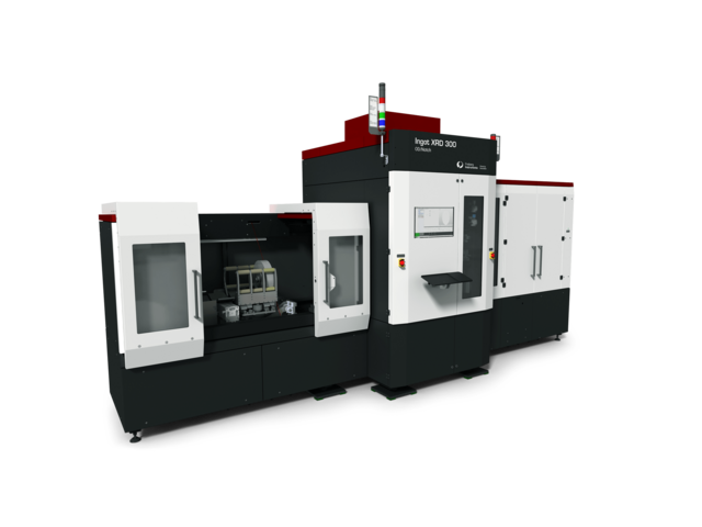
Skip breadcrumb navigation Breadcrumb Freiberg Instruments Products X-ray Diffraction Ingot XRD Ingot XRD OD/Notch Enables existing equipment to reach high-end OD/Notch specs for 200 mm and 300 mm ingots Interested? Get in touch! Contact now Product Sheet Skip menu Quick navigation Features Specifications Technology Software Contact Rethink your ingot grinding preparation: automated, precise, fast. Rapid determination of crystal orientation Optical geometry inspection with integrated confocal sensor Accurate and fully automated gluing and end piece attachment Features & Benefits 70–300 mm Ingot size 0.005° On-axis precision Flexible Loading and communication options Cylinder Calculation with hybrid metrology Cylinder Calculation with hybrid metrology Highest precision with high-speed measurement: < 5 secs/sample Typical standard deviation tilt (example: Si 100): < 0.003 °, minimum < 0.001 ° Automatic ingot alignment Automatic positioning of glue pieces Optical determination of geometric features (flat/notch position) of raw and/or grinded ingots Automatic marking of ingots Easy integration into process line (manual or robotic loading) Data Matrix Code (DMC) reader MES interface; SECS/GEM or similar up to 300 mm diamter and up to 520 mm lenght ingots Revolutionize your ingot grinding preparation with Ingot XRD 300 OD/Notch Discover the Key Advantages in 60 Seconds Ingot XRD 200 for 200 mm Ingots Ingot XRD 300 for 300 mm Ingots Interested? Our experts are happy to assist you. Get in touch! Contact us now! Specifications Parameter Standard deviation Diameter < 6 µm (grinded ingots); < 30 µm (raw ingots) Notch/Flat postion < 0.01° Notch depth < 6 µm Notch opening angle < 1.5° X-ray axis Vs. Flat/Notch position < 0.02° Ingot length > 0.1 mm Technologies Omega-scan Ultra-Fast Orientation Measurement for Single Crystals Learn more Software XRDStudio Multiple Operating ModesOperator Mode: Designed for fixed measurement parameters, ensuring a safe and streamlined workflow. Administrator Mode: Allows for the creation and modification of… Learn more Get in touch Do not hesitate to contact us – we are available to assist you with any inquiries or requests. Use our inquiry tool or reach out via email: sales @ freiberginstruments.com

Product

XRDmap Pro

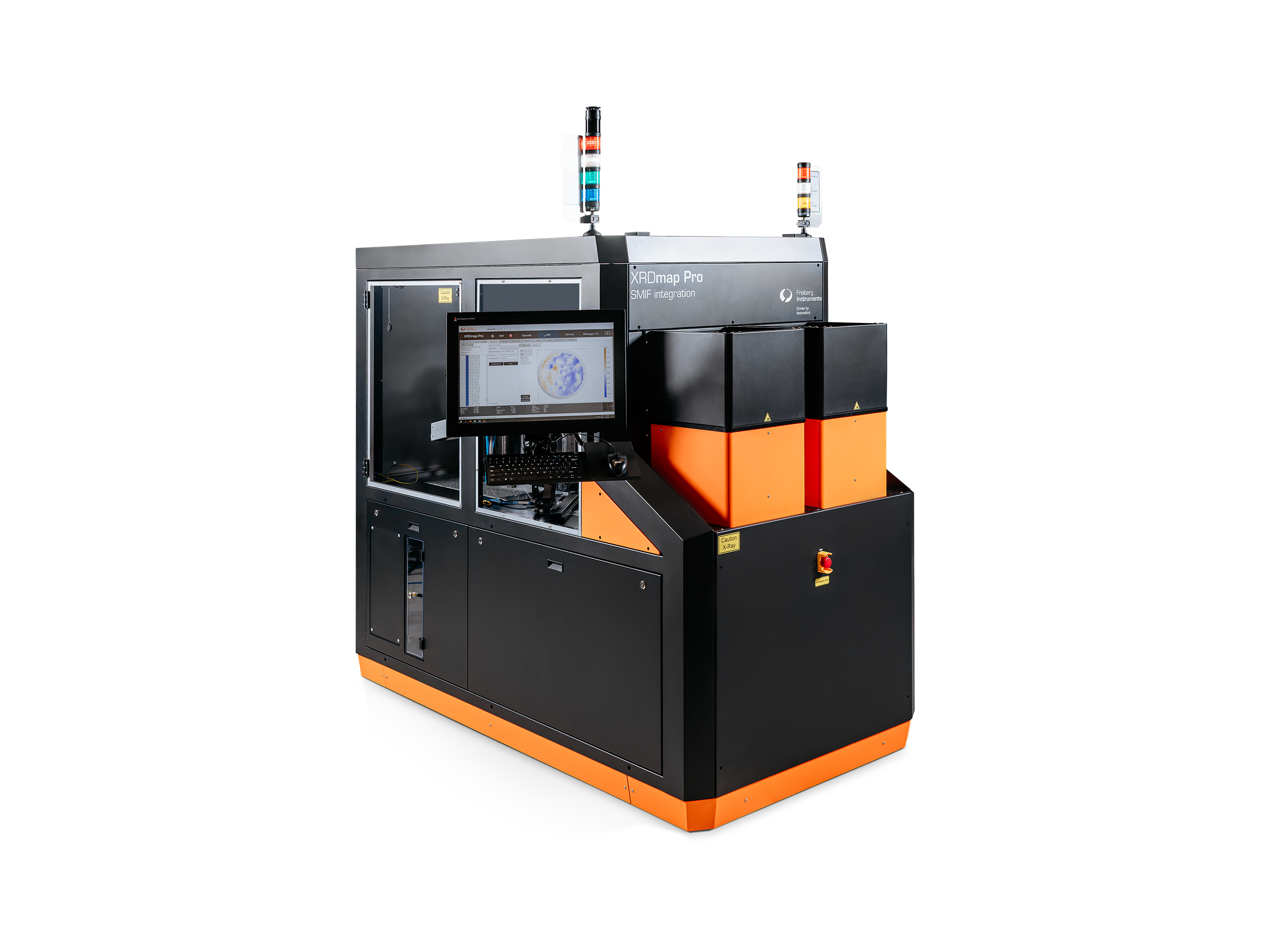
Skip breadcrumb navigation Breadcrumb Freiberg Instruments Products X-ray Diffraction XRDmap Pro XRDmap Pro Wafer Edition Inline wafer orientation mapping truly fab compliant Interested? Get in touch! Contact now Skip menu Quick navigation Features Applications Technology Software Contact Optimize wafer alignment inline for higher productivity. Ultra-fast hybrid X-ray optical metrology with proprietary algorithm Full automation featuring SMIF Loadports suitable for OHT connection Grows with your expansion: 70mm-230mm Wafersize flexibility Materials The XRDmap Pro Wafer Edition enables maximum value add by tuning subsequent processes such as epitaxy, lithography and implanting to the crystal orientation. This enables supplier process compliance and a smooth material flow by its ultra-fast measurement speed and seamless factory automation. Si Ge GaAs GaN Ga₂O₃ Diamond InP and more Features & Benefits 70–200mm Wafer Size 0.003˚ Offcut magnitude precision Flexible Loading and communication options Measured by opt. sensors Wafer Geometry Measured by opt. sensors Wafer Geometry Applications Crystal Surface Orientation Mapping Even within a single crystal, slight variations in crystal orientation can occur across the surface, often due to internal strains from lattice defects. Similarly, well-grown thin films can… Learn more Interested? Our experts are happy to assist you. Get in touch! Contact us now! Technologies Omega-scan Ultra-Fast Orientation Measurement for Single Crystals Learn more Software XRDStudio Multiple Operating ModesOperator Mode: Designed for fixed measurement parameters, ensuring a safe and streamlined workflow. Administrator Mode: Allows for the creation and modification of… Learn more Get in touch Do not hesitate to contact us – we are available to assist you with any inquiries or requests. Use our inquiry tool or reach out via email: sales @ freiberginstruments.com

Product

XRD-OEM

Skip breadcrumb navigation Breadcrumb Freiberg Instruments Products X-ray Diffraction XRD-OEM XRD OEM Fully automated in-line orientation and handling of ingots, boules, and pucks Exclusively through Malvern Panalytical Contact for demo Skip menu Quick navigation Features Applications Technology Software Contact Materials With XRD-OEM, a wide variety of materials can be precisely analyzed. Thanks to their flexibility and performance, our systems meet even the most demanding requirements. Si SiC GaAs and more Features & Benefits Ingots up to 450 mm diameter flat/notch detection large ingots Preset prior to sawing/grinding Ultra-fast crystal orientation measurement Ultra-fast crystal orientation measurement Ready for integration for any automation or processing system Designed for harsh environments (grinding, sawing) Compact, standard industrial interfaces Independent orientation measurement Measurements on flat surface or circumferences Optical notch detection Applications Orientation of silicon ingots: detection of flat and notch position prior to grinding diameter up to 8'' length up to 40 cm XRD-OEM – Exclusively through Malvern Panalytical This product is distributed by our trusted partner. Contact for demo Technologies Omega-scan Ultra-Fast Orientation Measurement for Single Crystals Learn more Theta-scan Precision X-ray Method for Single Crystal Orientation Learn more Software XRDStudio Multiple Operating ModesOperator Mode: Designed for fixed measurement parameters, ensuring a safe and streamlined workflow. Administrator Mode: Allows for the creation and modification of… Learn more XRD-OEM – Exclusively through Malvern Panalytical This product is distributed by our trusted partner. Contact for demo

Product

Ingot XRD SiC

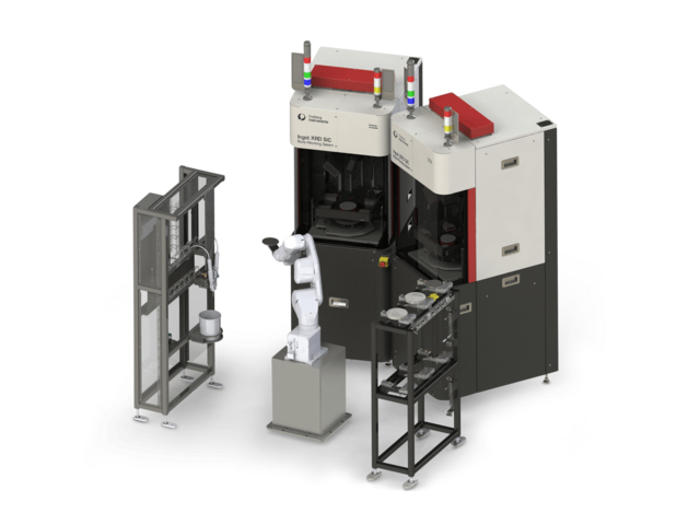
Skip breadcrumb navigation Breadcrumb Freiberg Instruments Products X-ray Diffraction Ingot XRD SiC Ingot XRD SiC Enables existing equipment to reach high-end OD/Notch specs. Interested? Get in touch! Contact now Skip menu Quick navigation Features Technology Software Contact Revolutionize your ingot post glueing preparation: Automated, precise and modular Ultra-fast hybrid X-ray optical metrology with proprietary algorithm Robot driven operations with modular metrology and tooling Advanced factory connectivity and service provisions Materials The Ingot XRD SiC delivers high-throughput and precision for the efficient production of advanced SiC wafers. SiC GaN AIN and more Features & Benefits Unmatched Quality with hybrid metrology 0.005˚ On-axis precision Flexible Loading and communication options Diameter 100–300 mm Diameter 100–300 mm Interested? Our experts are happy to assist you. Get in touch! Contact us now! Technologies Omega-scan Ultra-Fast Orientation Measurement for Single Crystals Learn more Software XRDStudio Multiple Operating ModesOperator Mode: Designed for fixed measurement parameters, ensuring a safe and streamlined workflow. Administrator Mode: Allows for the creation and modification of… Learn more Get in touch Do not hesitate to contact us – we are available to assist you with any inquiries or requests. Use our inquiry tool or reach out via email: sales @ freiberginstruments.com

Page

Luminescene dating, research, dosimetry

Luminescene dating, research, dosimetry Our R&D projects RAMSES-4-CE 04/2020 - 03/2024 Raman Absorption and eMission Spectroscopy in an intEgrated Sensor Circular Economy As a follow-up to the very successful InSPECtor project, Freiberg Instruments is developing a Raman sensor in this project. Together with the partner Helmholtz center Rossendorf HZDR and TU Bergakademie Freiberg and the Geological Survey of Finland GTK, the sensor will be implemented in a spectroscopy-based multi-sensor system for the recycling and re-mining industry. We focus on (1) the development of a Raman sensor unit, (2) the integration into the already developed LiF-HSI sensor system (inSPECtor) and (3) advanced data processing including multi-source data fusion and machine learning. The core innovation contributes to the digitalization of recycling streams. It allows for the identification of critical raw materials as well as energy stored in plastics as key inputs for simulations of energy and material cycles required for the transition towards a Circular Economy. Automated Lithium-Fluorid OSL Low-Dose-Measurement (ALFON) 2020/12/01 - 2021/11/30 The increasing use of ionising radiation in medical application (CT/X-ray; treatment) and other aspects of modern societies (radiation facilities, power plants), requires the active and passive measurement of radiation. This is paired with more and more stringent regulations on monitoring of radiation exposure and levels. Passive dosimeters are the most widespread and cheapest way to monitor the exposure to ionising radiation of large numbers of people. However, the widely used technique of film dosimetry was replaced by thermally stimulated luminescence (TL), which in turn is now out-phased in personnel dosimetry and slowly replaced by optically stimulated luminescence (OSL). New techniques require the development of new automated measurement equipment, e.g. myOSLraser. Especially dosimetry services, which are handling thousands of dosimeters every day, are faced with large costs of such transitions to new techniques, which are required to keep up with legislation and developments. This is accounted for in the ALFON project by the development of a 4-element OSL-dosimeter, which is shaped like the widespread used Panasonic 4-element TLDs, and thus will allow the continued use of peripheries for Panasonic TL-dosimetry with UD-readers in existing facilities. The artificial phosphors BeO and LiF are providing radiation responses close to human tissue and are therefore the material of choice in personnel dosimetry. The project aims to provide dosimeters and measurement equipment exceeding the requirements of EN/IEC 62387, especially on the detection of very low radiation doses. This will be the first commercial use of the new OSL material based on LiF (Sadel et al., 2019), and its favourable properties paired with the possibilities of 4 measurement positions in a single dosimeter, which opens many possibilities beyond the measurement of Hp0.07 and Hp10. In addition to develop optimized measurement conditions of the new material, the capacities for OSL-measurement are scaled up from the my OSLraser 2-element BeO reader (200 dosimeters), with automations for 500 and 4000 dosimeters. This requires 3-axle feeding mechanisms and a parallel line for dosimeters not meeting user or regulatory specifications, which have to be sorted out for inspection or re-measurement. The option to measure the same dosimeter again is special in OSL-dosimetry and not possible in TL-dosimetry, thus fulfilling the legal requirements in some countries.. The 2-element OSL-reader 'myOSLraser' for BeO is used as the basis of the development of the larger 4-element equipment. Reference: Sądel M, Bilski P & Kłosowski M (2019) Optically stimulated luminescence of LiF:Mg,Cu,P with different dopant concentrations. Radiation Measurements 123, 58-62. SISor - Sensor for Intelligent Sorting 2018/05/01-2020/04/30 The separation of waste, especially from electronic and electric devices (WEEE) is a topic, which has drawn a fast-growing interest on a global scale. Due to decreasing availability and rising production costs for raw materials such as rare earth elements (REEs) and precious metals, the mining of secondary resources from waste gained extremely in importance. In 2016, 44.4 million metric tons of e-waste were generated globally, an amount which is expected to increase steadily for the next decades. Within the SISor (Sensors for Intelligent Sorting) project the core aim is the development of an integrated sensor system for the automated detection of raw materials in the WEEE. An improved detection of valuable materials such as Au, Cu and rare earth elements would strengthen the sorting process of the e-waste, increasing the separation success tremendously. The consortium of the Helmholtz institute HZDR-HIF, the Canadian company Telops Inc. and Freiberg Instruments is going to develop a modular system, containing sensors based on hyperspectral mid-wave infrared (HS-MWIR) absorption spectroscopy and laser-induced fluorescence (LIF) emission spectroscopy. Both techniques are high-sensitive, non-invasive and can be optimized for fast-imaging. Thus, larger streams of recyclates could be processed more accurately in shorter time. This project is funded by the BMWi . inSPECtor - integrated Spectroscopy Sensor System The core aim of this project is to gather the respective partner competences to upscale an innovative product based on emission and absorption spectroscopy able to identify and map critical elements as rare earth elements in primary resources as drilling cores and secondary products. YouTube Here you can find external content of the provider Google LLC. To be able to display these, we need your consent. privacy policy Show provider content inSPECtor – integrated Spectroscopy Sensor System Development of measurement equipment for OSL-dosimetry with BeO 2016/03/15 - 2018/09/14 Personnel working in environments with potential exposure to artificial or increased radiation, like hospitals with CT/X-ray equipment, nuclear power plants, radiation facilities, etc., are required to be monitored for their radiation exposure. The availability of film material, which is one of the most important materials in such personal dosimetry, is not warranted on the long term. Other materials have been sought as possible replacements. The dependency of sintered BeO to radiation energy is close to tissue. Because of this favourable property, BeO is one of the phosphors of choice in personal dosimetry. Combined with the technique of Optically Stimulated Luminescence (OSL) for readout, BeO-OSL dosimetry is believed to supersede film dosimetry and at least to some extend thermoluminescence (TL) dosimetry. The projects aims towards the development of OSL-equipment (EN/IEC 62387) to efficiently read out a new 2-element BeO-OSL dosimeter (Hp07 and Hp10). The modular equipment provides the manual readout of a single BeO-dosimeter. An automation attachment provides the opportunity to measure batches of 20 dosimeters stored in magazines. A total of 10 of such magazines are located in a wheel, which is software driven for dosimeter measurement according to user definitions. In OSL dosimetry it is sufficient to measure part of the signal, which allows re-reading, for dose determination. This usually requires the zeroing before a dosimeter can be used again. Instead of a separate device the bleaching to zero will be achieved within the OSL-reader, which speeds up the process. For calibration purposes a special beta source for irradiation of the dosimeters is constructed. Some application require on-site immediate analysis (e.g. in a phantom) and dose determination. This will be achieved by a single-element BeO-OSL equipment, which is handheld and can be independently operated from batteries, providing immediate dose assessment. Reference Bos AJJ (2001) High sensitivity thermoluminescence dosimetry. Nuclear Instruments and Methods in Physics Research B 184, 3-28. READ 2016/06/01 - 2019/05/31 READ - R are EA rth ceramic phosphors for 3D optical readout D osimetry Dosimetry for radiation processing applications, as used e.g. in sterilization procedures for medical devices, is often tedious due to the constraints of quality assurance and fulfillment of the required standards (e.g. ISO 11137, ISO/ASTM 51204, 51608, 51649, …). It is moreover time consuming. As an industrial application it is desired to release irradiated products as quickly as possible. The project aims at the development of a handheld measurement device, which will provide instant dose information for user defined numbers of dosimeters attached to the product/product pallet, which will allow the immediate release if the specified requirements are met. While this can provide 3-D dose information based on the selected measurement spots, more details are sometimes required for product objects of very complex geometries, where it is essential to verify the dose at positions where dosimeters cannot be attached. For this purpose, a dosimeter material which can be sprayed onto surfaces and measured with a 3D-dose-scanner will be developed. The dosimetric properties of doped NaYF4 will be employed to develop dosimeters as labels and as spray. These ceramic phosphors exhibit an upconversion effect, denoting the transformation of long-wavelength (infrared or near-infrared) light into short-wavelength radiation (luminescence) with higher photon energy. Here, a dependency of the lifetime of the luminescence with dose (Figure 1) has been shown (Härtling et al., 2012; Reitzig et al, 2013; 2016). This allows the use of a broad dose range of few kGy to 150 kGy (Figure 2). Its high stability under ambient conditions corroborates the application of the material for industrial dosimetry, where the dose information is retained and readout is contactless. These properties make the material a promising candidate for optical dosimetry below 5 kGy, a dose range addressed so far only with more complex non-optical systems. Publication Christiane Schuster, Florent Kuntz, Alain Strasser, Thomas Härtling, Kay Dornich, Daniel Richter 3D relative dose measurement with a μm thin dosimetric layer, Radiation Physics and Chemistry, 2020,109238, ISSN 0969-806X Keywords: High dose dosimetry, Optical dosimetry, gamma irradiation, Electron beam irradiation, X Ray irradiation, ceramic phosphors, luminescence decay time, industrial radiation processing. Fig 1: Luminescence lifetime reduction after a 300 kGy electron irradiation (from Reitzig et al., 2016). Fig 2: Dose dependency of the luminescence lifetime of NaYF4 (from Reitzig et al., 2016). References Härtling, T., Reitzig, M., Mayer, A., Wetzel, C., Röder, O., Schreiber, J., and Opitz, J. (2012). Nondestructive testing of electron beam sterilization by means of an optically active marker material. In "Optical Components and Materials IX." pp. 825713-825713-6. Proceedings SPIE 8257. Reitzig, M., Goodband Rachel, J., Schuster, C., and Härtling, T. (2016). Optical electron beam dosimetry with ceramic phosphors as passive sensor material for broad dose ranges. tm - Technisches Messen 83, 171-179. Reitzig, M., Härtling, T., Winkler, M., Powers, P., Derenko, S., Toro, C., Röder, O., and Opitz, J. (2013). Time-resolved luminescence measurements on upconversion phosphors for electron beam sterilization monitoring. In "Smart Sensor Phenomena, Technology, Networks, and Systems Integration." (K. J. Peters, W. Ecke, and T. E. Matikas, Eds.), pp. 86930R-86930R-7. Questions? I'm here for you. Dr. Nadine Schüler Head of Research & Development +49 3731 419 540 LinkedIn profile Contact now Discover More Solutions Crystal Growth and Processing Learn more Epitaxial Layers & Thin Films Learn more Photovoltaic Learn more Luminescence Dating and Dosimetry Learn more

Page

Electrical semiconductor characterization

Electrical semiconductor characterization Our R&D projects SPV-4-UWBG – Development of Surface Photovoltage for ultra-wide bandgap semiconductors 2025/06/01 – 2027/12/31 The goal of this project is to establish the SPV measurement method for the first UWBG semiconductors, such as aluminum nitride, evaluate the method's validity, and interpret the measurements using alternative analysis techniques. Theoretical simulations will be performed to help to better understand the physical principles of the measurement principle. PERLE – Perovskite Tandem Solar Cells: Metrology for the PV Industry 2024/05/01 – 2027/04/30 In this project new methods for the inline characterization of Tandem solar cells based on MDP and SPS measurements are developed. Freiberg Instruments is working together with several research institutes and companies in this project to strengthen the German photovoltaic industry. Different layers and stacks of Perovskite and silicon are investigated and characterized. TemCrysT – GaN-Templates, GaN-Crystals and GaN-Wafers for the Development of GaN-Transistors 2023/07/01 – 2026/03/06 The aim of this project is to an automated characterization method for process control of GaN based on Raman measurements. This project aims to secure and expand the competitiveness of the semiconductor location Freiberg. For this purpose, Freiberg Instruments will develop a demonstrator for a fully automated confocal Raman measurement. This is used to analyze residual stresses, which naturally occur in the crystals due to the hetero-epitaxy process used. In this way, excellent feedback should be achieved along the entire process chain. In addition, the MDP method (microwave-detected photoconductivity), which has been established for silicon up to now, is to be applied to large HVPE GaN crystals for the first time and the possibilities of defect analysis on this material are to be researched and demonstrated. Furthermore, the capabilities of the newly developed SPV spectrometer (surface photovoltage) are to be adapted to GaN so that this device can be used for material characterization. G12 – Silicon mono-wafer development from M2 to G12: Cell geometries of the future 2022/04/01 – 2025/03/31 Development of the MDP lifetime measurement technology for monocrystalline bricks with a format of up to 210 x 210 mm The main goal of the "G12" project is the process and technology development of ingots and wafers with large format (formats (182x182 mm, 210x210 mm, possibly even 240x240 mm). The production of large ingots and large wafers requires further development of the crystallization systems, the process control, the mechanical processing of the ingot and bricks and ultimately also the qualification tools for the manufactured bricks and wafers. The focus of the sub-project at Freiberg Instruments is on the further development of lifetime measurements using MDP technology for large brick formats. Semicon 2021/03/01 – 2024/02/29 In this project a fast, contactless characterization tool based on THz is developed for the measurement of doping density, sheet resistance and layer thickness of thin semiconductor layers. SALSA – Measurement technology and sensitivity analysis for charge carrier selective solar cells 2021/04/01 – 2024/03/31 In the "SALSA" project, the inline measurement technology required for quality assurance and process control as well as quality assurance concepts are to be developed, optimized and techno-economically evaluated especially for progressive solar cell technologies such as the heterojunction route and the TOPCon route. The focus of Freiberg Instruments is on further development of their inline lifetime measurement abilities using MDP for HJT and TOPcon technology. The main tasks are: System optimization for TopCon and HJT (inline - MDPlinescan , offline - MDPmap ) Identification of suitable excitation conditions in different manufacturing stages (TOPCon / HJT) Detectability of defects in selected process stages Development of a concept for an optimized MDPlinescan system SPV – Development of a surface photovoltage spectrometer for the characterization of photoactive materials 2021/01/01 – 2022/12/30 So far, there are no universally applicable compact SPV spectrometers (SPV: surface photovoltage) available on the market with which practically any photoactive materials and semiconductors can be examined. The aim of this project is to develop a compact SPV spectrometer. With the help of our innovative SPV spectrometer and the measurement set-up for which a patent has been applied, charge separation, electronic transitions and diffusion lengths should be characterized contactless and with unprecedented sensitivity over a very broad spectral range from deep UV to near infrared. In accordance with the complementary strengths of the project partners, the focus of Freiberg Instruments is on device development and production of the demonstrator, of HZB on method development, development of critical components, validation and tests, and HZG on simulation and development of analysis and simulation software for SPV. Technology transfer PIDcon bifacial 2020/07/01 – 2020/12/31 In this project, the novel technology for testing bifacial solar cells for their sensitivity to potential-induced degradation ( PID ) is to be transferred from the Fraunhofer Center for Silicon Photovoltaics CSP to Freiberg Instruments GmbH and adapted into a marketable product. The Fraunhofer CSP has applied for a patent for a novel process (process and arrangement for testing solar modules or solar cells for potential-induced degradation) and will transfer this knowledge to Freiberg Instruments. This project is funded by SAB and the EU. QualiZell mess-ODNP 2019/11/01 – 2021/10/30 In cooperation with the technical university Bochum, Freiberg Instruments is developing a tool for ODNP measurements, a combination of EPR and NMR for the investigation of water dynamics and protein function. This project is funded within the ZIM network “Qualitätskontrolle Zelltherapie” (https://www.qualitaetskontrolle-zelltherapie.de/) by ZIM and the German government. µTHIN 2019/09/01 – 2021/08/31 The objective of this project is to develop a sensor for sheet resistance measurements on thin films of e.g. GaN on Si via microwave detection. Furthermore, the MDP technology will taken to its next level concerning the time resolution, sensitivity and mapping possibility at different temperatures. The project partner the technical university Freiberg, is correlating the results of the new sensor and the improved MDP with PL and Raman measurements to gain new insights in the interpretation of the measurements results. This project is funded out of the EFRE fond of the EU. Omega-Scan 2018/01/01 – 2020/12/31 Advancement of Omega-Scan technology for different applications Freiberg Instruments is further advancing its Omega-Scan technology for orientation of single crystals for different applications as orientation of diamond and other wide bandgap semiconductors, epitaxial layers, turbine blades and quartz. The project is funded by the SAB and the EU. PIDrecovery 2018/01/01 – 2020/12/31 Freiberg Instruments takes part in a project with the goal to develop a method to predict PID recovery and hence the efficiency of a module. Freiberg Instruments is further developing its tool PIDcheck for the PID test of modules in free field and its recovery. The project is funded by BMWi . Smart3 | materials – solutions – growth 2017/05/01 – 2020/04/30 Smart processes – process technology for smart materials MSM-production and material characterization Freiberg Instruments is investigating the applicability of x-ray diffraction methods for crystallographic orientation determination on MSM single crystals (Magnetic Shape Memory) in subproject 2 "Process chains for the production of MSM actuator sticks". In the case of a positive evaluation, the closer connection to the subsequent processing steps will be examined and the determination process will be automated. The project is funded by the BMBF within the Funding project “Zwanzig20”. Q-Crystal 2017/01/01 – 2019/12/31 The overall objective of this project is to optimize the production processes of block silicon under industrial conditions with the help of fast and novel methods of quality assessment of bricks and wafers and thus to increase the quality of silicon wafers produced therefrom. This is to be demonstrated by a highly efficient industrial solar cell structure. Freiberg Instruments cooperates in this project with 7 partners from industry and Fraunhofer society. This project is funded by BMWi . Contact person: Dr. Nadine Schüler (schueler@freiberginstruments.com) SEA4KET 2013/11/01 – 2017/04/30 The aim of this project is the evaluation of different metrology components for 450 mm wafers. Freiberg Instruments is delivering a measurement head for high resolution lifetime measurements in this project. CUT-B 2015/12/01 – 2018/11/30 The objective of this project is to evaluate and improve the cutting edge characterization and technology for the german photovoltaic industry. The main focus are inline metrology tools and the prediction of solar cell efficiency by means of different measured parameters. Freiberg Instruments is involved in this project with its inline metrology tool MDPinline. The aim is to improve the possibilities of solar cell efficiency prediction via lifetime measurements on wafers after different process steps. Further more typical errors in different process steps are investigated to enable an automatic detection. This project is supported by BMWi . Contact person: Dr. Nadine Schüler E-Mail: schueler@freiberginstruments.com WIDE 2016/01/01 – 2018/12/31 This project involves Freiberg Instruments and the TU Freiberg and has the goal to improve the scientific tool MDPmap for the measurement of wide bandgap semiconductors. This includes Improvement of the time resolution, in order to be able to measure also small lifetimes (> 10 ns) Improvement of the sensitivity Enhancement of temperature range up to 800 K for the investigation of deep defects This project is funded by SAB and the EU. PIDcheck 2016/03/07 – 2017/06/06 This is a funded technology transfer project, in which Freiberg Instruments in cooperation with the Fraunhofer Institute CSP in Halle is developing a PID test tool for the test of modules in free field. This project is funded by the SAB and the EU. Questions? I'm here for you. Dr. Nadine Schüler Head of Research & Development +49 3731 419 540 LinkedIn profile Contact now Discover More Solutions Crystal Growth and Processing Learn more Epitaxial Layers & Thin Films Learn more Photovoltaic Learn more Luminescence Dating and Dosimetry Learn more

Page

Reference list – TL/OSL reader

Reference list – TL/OSL reader Indian subcontinent Ass.-Prof Dr Manoj Kumar Jaiswal, Department of Earth Sciences, Indian Institute of Science Education and Research, Kolkata, India Dr Manoj K. Rathore, M.P. Council of Science and Technology, Bhopal, India Prof Dr Milap Chand Sharma, Centre for the Study of Regional Development, Jawaharlal Nehru University, New Delhi, India Dr Babita Tiwari, Technical Physics Division (TPD), Bhabha Atomic Research Centre (BARC), Mumabi, India Dr Meghnath Sen, Radiation Safety Systems Division (RSSD), Bhabha Atomic Research Centre (BARC), Mumabi, India Dr Ramanathan Bhavani, TL/OSL Laboratory, Geological Survey of India, Faridabad, India Mr Md. Hossain Khasru and Mr Abdul Baquee Khan Majlis, Geological Survey of Bangladesh, Dhaka, Bangladesh Africa Prof Nabil El-Faramawy, Faculty of Science, Nuclear and Radiation Physics, Ain Shams University, Cairo, Egypt Asia Mr Mohd Sairul Bin Ramle and Mr Ahmad Fadly Bin Jusoh, Pusat Penyelidikan Arkeologi, Universiti Sains Malaysia, Penang, Malaysia Mr En. NorFaizal, Agensi Nuklear Malaysia (Nuklear Malaysia), Kajang Selangor, Malaysia Prof Anchuan Fan, Department History of Science and Scientific Archaeology, University of Science and Technology of China, Hefei, China Ass.-Prof Dr Shibiao Bai, School of Geography Science, Nanjing Normal University, Nanjing, China Dr Weiming Liu, Institute of Hazards and Environment, Chinese Academy of Sciences, Chengdu, China Ms Liu Yang, Institute of Geographical Sciences of Henan Academy of Sciences, Zhengzhou, China Prof Liping Zhou, Department of Geomorphology and Quaternary Geology, College of Urban and Environmental Sciences, Peking University, Beijing, China Prof Xulong Wang and Dr. Shugang Kang, Institute of Earth Environment, Chinese Academy of Sciences, Xi’an, China Ms Wang, Institute of Hydrogeology and Environmental Geology (IHEG), Chinese Academy of Geological Sciences (CAGS), Beijing, China Dr Ma Wei, College of Chemical and Environmental Engineering, Pingdingshan University, Henan, Pingdingshan, China Ms Yang Hui, Institute of Karst Geology, Chinese Academy of Geological Sciences (Karst-CAGS), Guangxi, Guilin, China Dr Toru TAMURA, Marine Geo-Environment Research Group, Research Institute of Geology and Geoinformation, Geological Survey of Japan, National Institute of Advanced Industrial Science and Technology (AIST), Japan Dr Kazumi ITO, Geodynamics Research Group, Research Institute of Earthquake and Volcano Geology, Geological Survey of Japan, National Institute of Advanced Industrial Science and Technology (AIST), Japan Mr Eiji NIKATA, Geophere Science Sector, Civil Engineering, Research Laboratory, Central Research Institute of Electric Power Industry (CRIEPI), Japan Dr Jin Cheul Kim, Surficial Environment & Global Change Department, Korea Institute of Geoscience and Mineral Resources, Korea Mr Jin Myung Kim, Dating Analysis Services Company, Radpion, Korea KFDA (Korean Mininstry of Food and Drug Safety), Gyeongin Regional Office, Korea KFDA (Korean Mininstry of Food and Drug Safety), Seoul Regional Office, Korea Prof Majid Nabi-Bidhendi and Dr Morteza Fattahi, Institute of Geophysics, University of Tehran, Tehran, Iran Prof Dr Mustafa Topaksu, The Faculty of Arts and Sciences, Cukurova University, Adana, Turkey Dr Berna Yildirim, Physical Analysis Laboratory, Tekirdağ Food Control Laboratory Directorate, (Ministry of Food, Agriculture and Livestock), Tekirdağ, Turkey Dr Berrin DİNÇER, Ankara Food Control Laboratory Directorate, Republic of Turkey Ministry of Food Agriculture and Livestock, Ankara, Turkey Dr L.S. Arun Kumar, Medical Physics and Radiation Protection, DGEA, Ministry of Health, Muscat, Sultanate of Oman Prof Leonid Oster, Head of Physics Unit, Shamoon College of Engineering, Israel Dr Chalermpong Polee, Thailand Institute of Nuclear Technology Nuclear Research and Development Division, Nakhon Nayok, Thailand Mr. Weerachat Wiwegwin, Environmental Geology Division, Department of Mineral Resources, Thailand Americas Dr Sebastien Huot, Illinois State Geological Survey, Natural Resources Building, University of Illinois, Champaign, USA Ass.-Prof Luiz G. Jacobsohn, Department of Materials Science and Engineering, COMSET - Center for Optical Materials Science and Engineering Technologies, Clemson University, Anderson, USA Mr Serge Fayeulle, Artemis Testing Lab, Louisville, Colorado, USA Dr Jose Luis Antinao, Indiana Geological Survey, Bloomington, Indiana, USA US Navy, United States of America Dr Shannon Mahan, Geosciences and Environmental Change Science Center, U.S. Geological Survey, Unites States of America Mr Srinivas Sista, GE Healthcare, Wisconsin, United States of America Prof Michel Lamothe, Département des sciences de la Terre et de l'atmosphère, Université du Québec à Montréal, Montréal, Canada Dr Jesus Roman Lopez, Laboratorio de Dosimetria de la Unidad de Irradiacion y Seguridad Radiologica, Instituto de Ciencias Nucleares UNAM, Mexico City, Mexico Dr Helen Jamil Khoury, FACEPE, Recife, Brazil Dr André Oliveira Sawakuchi, Instituto de Geociências, Universidade de São Paulo, São Paulo, Brazil Mr Luiz Carlos Oliveira, University of Sao Paulo, Ribeirao Preto, Brazil Australia and Oceanica Prof Richard (Bert) Roberts, School of Earth and Environmental Science, University of Wollongong, Wollongong, Australia Dr Prabhakar Ramachandran, Princess Alexandra Hospital, Brisbane, Australia Europe Dr Norbert Mercier, Maison de l ' Archéologie, Université Bordeaux Montaigne, Pessac Cedex, France Dr Antoine Zink, Centre de recherche et restauration des musées de France, Palais du Louvre-Porte des Lions, Paris, France Dr Armel Bouvier, Responsable du département archéologie, CIRAM, Martillac, France Ass.-Prof Magali Rizza, CEREGE - OSU Pytheas, Aix-Marseille Université, Marseille, France Dr Emmanuel Vartanian, Re.S.Artes , Bordeaux, France Dr Phillip Toms, School of Natural & Social Sciences, University of Gloucestershire, Cheltenham, United Kingdom Dr Jean-Luc Schwenninger, Research Laboratory for Archaeology and History of Art, University of Oxford, Oxford, United Kingdom Dr Julia Katzmann, Fraunhofer Institute for Ceramic Technologies and Systems IKTS, Dresden, Germany Prof Dr Markus Fuchs, Institut für Geographie, Justus-Liebig-Universität Gießen, Gießen, Germany Dipl.-Geogr. Alexander Fülling, Geographisches Institut, Humboldt-Universität, Berlin, Germany Dr Tobias Lauer, Department of Human Evolution, Max Planck Institute for Evolutionary Anthropology , Leipzig, Germany Dr Clemens Woda, Institute of Radiation Protection, Helmholtz Zentrum München, Munich, Germany Dr Nicole Klasen, Geographisches Institut der Universität zu Köln, Cologne, Germany Dr Christoph Schmidt, Lehrstuhl für Geomorphologie, Universität Bayreuth, Bayreuth, Germany Prof Dr Frank Preusser, Institute of Earth and Environmental Sciences - Geology, University of Freiburg, Freiburg, Germany PD Dr Michael Scholz, GSI Helmholtzzentrum für Schwerionenforschung GmbH, Darmstadt, Germany Dr Sumiko Tsukamoto, Department of Geochronology and Isotope Hydrology, Leibniz Institute for Applied Geophysics, Hannover, Germany Eurofins NDSC Food Testing Germany GmbH, Hamburg, Germany Bundesamt für Strahlenschutz, Oberschleißheim, Germany LMU Klinikum, Munich, Germany Mr Braun, Universitätsklinikum Hamburg-Eppendorf, Hamburg, Germany Labor Kotalla GbR, Haigerloch, Germany Dr Eduardo Gardenali Yukihara, Paul Scherrer Institut, Villigen PSI, Switzerland Dr Jorge Sanjurjo Sánchez, University Institute of Geology, University of A Coruña, Spain Dr Natacha Gribenski, Department of Physical Geography and Quaternary Geology, Stockholm University, Stockholm, Sweden Dr Liliana Stolarczyk, Department of Medical Physics, Institute of Nuclear Physics PAN, Cracow, Poland Prof Dr Eugeniusz Zych, Faculty of Chemistry, University of Wroclaw, Wroclaw, Poland Dr hab. Dariusz Hreniak, Department of Excited State Spectroscopy, Institute of Low Temperature and Structure Research, Polish Academy of Sciences, Wroclaw, Poland Dr Artur Ginter, Thermoluminescence and Spectrometry Laboratory, Institute of Archaeology, University of Lodz, Poland Ms Klaudia Kucińska, National Centre for Radiation Protection in Health Care, Lodz, Poland Prof Dr Andreas Lang and Dr Michael Discher, University of Salzburg, Department of Geography and Geology, Salzburg, Austria Mr Roman Truneček and Ms Veronika Olšovcová, ELI beamlines, Dolní Břežany, Czech Republic Hungarian Academy of Sciences Centre for Energy Research, Radiation Protection Department, Budapest, Hungary Dr Laima Trinkler, University of Latvia, Institute of Solid State Physics, Riga, Latvia
Page

Freiberg Instruments

Driving efficiency and accuracy with our automation and metrology expertise Bringing Innovation from Lab to Fab At Freiberg Instruments, we drive technological advancements by developing high-precision measurement and automation solutions that set new industry benchmarks. Our systems enable leading companies and researchers to enhance their processes and gain reliable data for breakthrough innovations. With over 3,000 metrology systems installed worldwide , we serve industries such as microelectronics, semiconductors, photovoltaics, chemicals, and medical technology. Our dedication to quality—certified according to ISO 9001:2015 – makes us a trusted partner for future-driven solutions. Our goal: transforming innovation from the lab into industrial applications—efficiently, precisely, and sustainably. Learn more about us Cutting-edge Metrology Solutions for Various Applications Crystal Growth and Processing Our advanced X-ray diffraction (XRD) systems optimize grinding and sawing processes, ensuring perfect alignment for high-performance semiconductor applications. Discover more Epitaxial Layers and Thin Films Our non-destructive metrology tools provide critical insights into wafer properties, layer thickness, and defect detection. Discover more Photovoltaic Our advanced tools support high-speed, high-accuracy analysis of wafers and thin films, ensuring optimal yield and production performance. Discover more Luminescence Dating and Dosimetry Our instruments provide unparalleled sensitivity and reliability in geochronology and dosimetry applications. Discover more Radiation Monitoring Our solutions provide real-time monitoring, ensuring compliance and protection in critical industrial and research environments. Discover more Research and Development Our advanced metrology tools support material research, semiconductor development, and defect analysis with maximum accuracy. Discover more Precision Redefined: Discover Our Advanced Metrology and Automation Solutions XRD series Advanced X-Ray diffractometers Devices for crystal orientation, sample alignment & quality control Learn more RES series Resistivity Mapping Accurate material analysis for semiconductor quality control Learn more MDP series Microwave Detected Photoconductivity Contactless mapping of key electrical semiconductor parameters Learn more SPS/SPV series Surface Photovoltage Spectroscopy Contactless characterization of key electro-optical material parameters Learn more DPM series Double Prism Monochromator Unlock the future of spectral analysis Learn more PID series Potential Induced Degradation Advanced Solutions for PID Detection and Quality Control in Solar Cells & Module Learn more TL/OSL series Luminescence Dating and Dosimetry Advanced luminescence systems for geology, archaeology, and radiation dosimetry Learn more RMS series Radiation Monitoring System Protecting people, workspaces, and the environment with precision Learn more Ramses series Raman Sensor Fully automated, high sensitive for polymer and semiconductor sorting Learn more We are driven by Innovation. Freiberg Instruments constantly redefines the limits. Excellence in Automation and Metrology is our core motivation. Dr. Kay Dornich CEO Services for Your Success From tailored solutions to expert training and responsive technical support, our services are designed to keep your operations running smoothly and efficiently. Discover our services Customization Automation Research and Development Training and Application Expertise Technical Support Latest News 11/05/2024 HZB patent for semiconductor characterisation goes into serial production 12/07/2023 Collaboration Announcement: Freiberg Instruments and Ajuba 11/21/2023 A precision better than 1% is achievable with lexsygsmart luminescence reader More News Upcoming Events More Events Driving Innovation with You Our team of engineers, scientists, and professionals shares a relentless passion for excellence. Together, we have built a reputation for reliability, innovation, and exceptional customer service. We constantly redefines the limits of metrology. Meet the Team Career Opportunities Thesis and Internship Discover more About Freiberg Instruments Get to know us We assist you with any inquiries or requests Contact us