Found 271 results in 2 milliseconds.

Product

Beta-Aerosol monitor

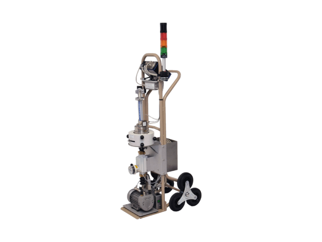
Skip breadcrumb navigation Breadcrumb Freiberg Instruments Products Radiation Monitoring Systems Beta-Aerosol monitor Beta-Aerosol monitor A portable device with 50 mm PIPS detector; ISO 11929 compliant concentration calculation Interested? Get in touch! Contact now Skip menu Quick navigation Features Contact Features & Benefits Determination of the concentration of radioactive beta aerosols/particulates by enrichment on HEPA filters Mobile beta aerosol monitors for workplace monitoring in nuclear facilities and laboratories Calculation of the concentration in accordance with DIN ISO 11929 Radon Compensation Detector Beta and alpha sensitive ion-implanted PIPS detector with 2000 mm 2 active detector area Light-tight detector, protected with changeable foil agains contaminations State-of-the-art electronics Low noise charge sensitive preamplifier Proven SMC 2100 / DA with one amplifier each for beta and alpha 3 separate measurement windows for beta and alpha artificial as well as alpha natural 7 “TFT color display with touch functions, resolution 800 x 480 pixels, swiveling Storage of relevant measurement results on microSD card, readable via USB Recorder output, potential-free relay outputs, signal lights and differential pressure monitoring Rotary vane vacuum pump and quantometer for determining throughput Get in touch Do not hesitate to contact us – we are available to assist you with any inquiries or requests. Use our inquiry tool or reach out via email: sales @ freiberginstruments.com
Product

SmartRAY2

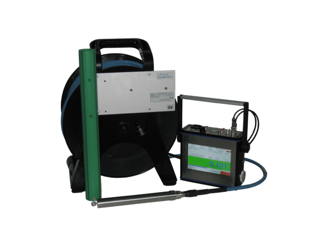
Skip breadcrumb navigation Breadcrumb Freiberg Instruments Products Radiation Monitoring Systems SmartRAY2 SmartRAY2 High range dose rate meter Interested? Get in touch! Contact now Skip menu Quick navigation Features Contact Features & Benefits Probe use of a selected gamma ionization chamber suitable for its gamma sensitivity for the measurement of gamma dose rate and dose 10 decades measuring range for the gamma dose rate stainless steel housing for the gamma ionization chamber, suitable for an underwater use down to 40 m depth pluggable waterproof cable connection on the stainless-steel housing, mono-cable connection between stainless steel housing and cable drum possible use of ionization chambers with different gamma sensitivities for the shift of the 10-decades measuring range State-of-the-art electronics in operation proven SMC 2100 measuring technique with current-to-frequency converter, integrated in the SmartRAY2 housing SmartRAY2 with serial interface RS485 for a PC connection 7“ color display with touch functions, resolution 800x480 pixels integrated in the SmartRAY2 housing storage of the measured values on MicroSD card readout of the measured values via USB connection connections for relays, signal lights and external start signal output of the measured value as analog 0-20mA current signal mains or battery pack operation, accumulator charging at mains operation, energy management for battery pack control cable drum for probe connection on long cables up to 60 m Get in touch Do not hesitate to contact us – we are available to assist you with any inquiries or requests. Use our inquiry tool or reach out via email: sales @ freiberginstruments.com
Product

SmartKONT

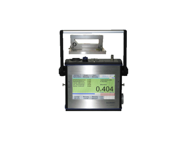
Skip breadcrumb navigation Breadcrumb Freiberg Instruments Products Radiation Monitoring Systems SmartKONT SmartKONT Radiation contamination monitor Interested? Get in touch! Contact now Skip menu Quick navigation Features Software Contact Features & Benefits Measuring device for the connection of beta + alpha or alpha sensitive proportional detectors, such as HGZ / RGZ 200-T. Measurement results with decision aids conforming to DIN ISO 11929. rugged aluminium housing with 7“ colour display (resolution 800 x 480 pixels) and touch functions SMC 2100 measuring technique proven in use with serial RS 485 interface for PC connection switchable loudly puIse acoustic, headphone jack storage of measurement results on Micro SD card readout of measurement values via USB connection mains or battery pack operation, accumulator charging during mains operation energy management for battery pack monitoring external Start and Storage button, release via. infrared or cable button Interested? Our experts are happy to assist you. Get in touch! Contact us now! Software detection of the results DIN ISO 11929 conform contamination or release measurements automatic determination of requested measuring time single measurement or rate meter Alpha+Beta and Alpha measurements displayed results cps or Bq/cm2 selectable recurrent examination support storage of measuring values with comments device, measurement and calibration parameters free selectable Windows software AM-SMCA01 Get in touch Do not hesitate to contact us – we are available to assist you with any inquiries or requests. Use our inquiry tool or reach out via email: sales @ freiberginstruments.com
Product

Comet2500

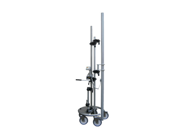
Skip breadcrumb navigation Breadcrumb Freiberg Instruments Products Radiation Monitoring Systems Comet2500 Comet 2500 Spatially resolved detector rod for shipping container measurement Interested? Get in touch! Contact now Skip menu Quick navigation Features Specifications Contact Features & Benefits Detector rod with gamma sensitive Geiger Müller tubes Local resolution through a serial line-up of 8 identical GM tubes Uniform sensitivity over the total length of the detector rod High gamma sensitivity for Co-60 with 18 cps per µSv/h Time saving and effective dose rate screening of transport containers Radioactivity check of floors and walls Track-down of “hot spots“ over a length of 2.5 m Technique 2 reliable Serial Micro Channels (each of variation SMC/QD) integrated in the detector rod Modular movable design with display and height adjustable detector rod High flexibility in its applications through vertical and horizontal positions of the detector rod Portable display und detector rod, simply with one hand (without tripod) 7“ color display with touch functions, resolution 800 x 480 pixels Distance measurement with laser meter mains or battery pack operation, accumulator charging at mains operation, energy management for battery pack control Get in touch Do not hesitate to contact us – we are available to assist you with any inquiries or requests. Use our inquiry tool or reach out via email: sales @ freiberginstruments.com

Page

Events

Events More Events

Technology

Omega-scan

Omega-scan Ultra-Fast Orientation Measurement for Single Crystals Advantages of the Omega-Scan Method Stable and Simplified Setup The X-ray tube and detector remain fixed, requiring only a single measuring circle and no monochromator. Comprehensive Data Collection All necessary data for full orientation determination is captured in just one rotation. High Precision with Minimal Measurement Time The method delivers exceptional accuracy within a short measurement duration. These features make the Omega-Scan method particularly well-suited for routine measurements and industrial applications, where speed and reliability are essential. Understanding the Omega-Scan Method The Omega-Scan technique involves rotating the specimen 360° around a specific axis, such as the surface normal. The X-ray source and detector are positioned based on the crystal type to ensure an optimal number of reflections per turn. By analyzing the angular positions of these reflections, the crystal lattice orientation is determined in relation to the rotation axis. To precisely align the lattice orientation with the crystal surface, a laser beam checks the surface direction. Other relevant reference planes or directions can also be measured using optical tools. This technique enables accurate orientation measurement of single crystals in any configuration, achieving a reproducibility within a few arc seconds—often in just a few seconds of measurement. A specialized application of the Omega-Scan method is precision lattice-parameter determination , particularly for cubic crystals, providing highly accurate structural insights. Related Applications: Crystal Surface Orientation Mapping , 3D Mapping of Crystalline Turbine Blades , Quartz Bar Aligning , Automatic Wafer Sorting , Quartz Blank Sorting , Samples with a wide variety of geometry & size , Marking and measuring of in-plane directions , Crystal quality , NLO Materials: Crystal Quality & Optical Axis Orientation Matching Products XRD series Ingot XRD Enables existing equipment to reach high-end OD/Notch specs for 200 mm and 300 mm ingots Learn more XRD series Wafer XRD for fully automated sorting, sample crystalline orientation, sample dimension, optical notch/flat and edge profile determination and more Learn more XRD series Omega/Theta XRD for ultra-fast crystal orientation, crystal alignment in production, quality control, rocking curve measurements, material research and more Learn more XRD series DDCOM Ultra-fast, bottom surface measuring crystal orientation in a compact package Learn more XRD series SDCOM Ultra-fast, top surface measuring crystal orientation in a compact package Learn more XRD series XRD-OEM Fully automated in-line orientation and handling of ingots, boules, and pucks Learn more XRD series Ingot XRD SiC Enables existing equipment to reach high-end OD/Notch specs. Learn more XRD series Quartz Bar XRD Enable tight frequency specs in mass production Learn more XRD series Quartz Wafer XRD Enable tight frequency specs in mass production Learn more XRD series Quartz Blank XRD Enable tight frequency specs in mass production Learn more XRD series XRDmap Pro Inline wafer orientation mapping truly fab compliant Learn more XRD series Angle Sorter This product launching soon Learn more Get in touch Do not hesitate to contact us – we are available to assist you with any inquiries or requests. Use our inquiry tool or reach out via email: sales @ freiberginstruments.com

Technology

Minority carrier lifetime

Minority carrier lifetime The minority carrier lifetime is one of the most important and significant material parameters. It i Minority carrier lifetime The minority carrier lifetime is one of the most important and significant material parameters. It is extremely sensitive to smallest amounts of impurities or intrinsic defects and hence an ideal parameter for inline characterization of material quality and process control. It is of essential importance for the performance of many semiconductor devices. The minority carrier lifetime is defined as the average time it takes an excess minority carrier to recombine. It is strongly dependent on the magnitude and type of recombination processes in the semiconductor. The main different types of recombination are: SRH recombination ⇒ via defects Auger recombination ⇒ via a three particle process intrinsic or radiative recombination ⇒ via band to band \(\cfrac{1}{\tau_{bulk}} =\cfrac{1}{\tau_{SRH}} + \cfrac{1}{\tau_{Auger}} + \cfrac{1}{\tau_{rad}}\) For silicon SRH is often the dominant recombination mechanism. The minority carrier lifetime in the bulk depends accordingly on the number of defects present and on their recombination properties. In silicon the lifetime can be as high as 1ms, where as in a direct semiconductor as GaAs, where the intrinsic recombination is dominant, the lifetime is only in the range of ns...µs. Besides the defect properties the minority carrier lifetime is dependent on the injection level (excess carrier concentration) and the doping concentration. Figure 1 and 2 display this dependencies for all different lifetimes. Fig. 2: injection dependence of all important recombination rates Fig. 3: doping dependence of all important recombination rates The measured effective lifetime is composed of the bulk lifetime and surface lifetime, which depends on the surface properties of a sample. Hence the surface has to be passivated, if you want to measure the bulk properties of your sample. If you want to investigate the surface passivation quality a FZ-Si wafer is recommendable, because the bulk recombination can be neglected. \(\cfrac{1}{\tau_{eff}} = \cfrac{1}{\tau_{bulk}} + \cfrac{1}{\tau_{surface}}\) Besides that the measured effective lifetime is dependent on the measuring method. For more details read: [1] S. Rein, Lifetime Spectroscopy - A Method of Defect Characterization in Silicon for Photovoltaic Applications, Vol. 85 (Springer, Berlin Heidelberg, 2005) [2] D. K. Schroder, Semiconductor Material and Device Characterization, 2 ed. (John Wiley & Sons, New York, 1998) Matching Products MDP series MDpicts pro High-Resolution, Temperature-Dependent Lifetime Measurement System for Precise Material Characterization Learn more MDP series MDPpro 850+ Advanced Solution for Quality Control of Monocrystalline Silicon Ingots, Bricks, and Wafers Learn more MDP series MDPlinescan Versatile OEM Unit for Lifetime Measurements on Silicon Samples, from Bricks to Processed Wafers Learn more MDP series MDpicts Temperature-Dependent Lifetime Measurement System for Advanced Material Analysis Learn more RES series RESmap High-Precision Resistivity Mapping System for Accurate Material Analysis Learn more MDP series MDPmap Precision Lifetime Charachterization with Exceptional Sensitivity Learn more MDP series MDPspot Quick and Simple Lifetime Measurement Made Easy Learn more Get in touch Do not hesitate to contact us – we are available to assist you with any inquiries or requests. Use our inquiry tool or reach out via email: sales @ freiberginstruments.com

Technology

Conductance Test and Power Loss

Conductance Test and Power Loss The conductance test and power loss are used to determine the pass/fail criteria for the PID test In order to establish an easy way to decide whether a solar cell or mini-module has a PID problem or not, even though the operator itself has not the physical background the power loss is determined and given as an output by the software PIDStudio. It shows the expected relative power loss of the degraded area of the cell under STC (1000 W/m 2 ) ∆P: Absolute power loss P 0 : Nominal power under standard test conditions (STC) = 1000 W/m 2 irradiance ∆P/P 0 : Relative power loss under STC conditions (approximate value, valid for power loss up to ~30%) V mpp : Voltage at maximum power (= 0.5 V for standard silicon solar cells) I mpp : Current at maximum power (= 8 A for standard silicon solar cells at STC) R p : Measured parallel resistance (= V/I as measured between front and back contact for the whole cell) A cell : Cell area (= 243 cm² for standard silicon solar cells) A pid : PID-tested area (= 100 cm² for standard PIDcon setup) Furthermore an easy pass or fail criterion after finishing the PID measurement is suggested. It is assumed that an efficiency loss of 3% at the end of the PID test lead to a fail of the solar cell (according to IEC-Standard). The measurement time therefore is 168 h at room temperature or 72 h at 85 °C (recipe “Long”). An efficiency loss of 3% is equal to an increase of the cell’s conductance of 150 mS for the tested area, meaning 1.5mS/cm 2 related to the 100 cm 2 electrode size. The formula for calculating the conductance is as follows: So it is the reciprocal of the parallel resistance related to the degraded area. If the PID diagram of a cell after 72 h shows a higher conductance increase as 1.5 mS/cm 2 , it fails the test and has a PID problem and should be sorted out, otherwise it will pass it. Please keep in mind that the test is not for absolute value of conductance, but only for increase of conductance (Conductance at the start point is unequal to zero). Please notice that the curves “Power loss” and “Conductance” look equal in the auto focus option, since the formulas are comparable. To save measurement time, the recommended measurement time is shortened to 4 hours. The fail criterion for that time span is 0.1 mS/cm 2 at 1000 V and 85 °C. Keep in mind that this criterion is only a hint for a PID problem, a conductance increase of 0.1 mS/cm 2 in 4 h will not lead to a measurable power loss. Therefore it is in the customer’s responsibility to check and use this fail criterion. Same applies for the recipe “Fast” with a fail criterion of 0.025 mS/cm 2 after 1 h. Nevertheless usage of higher measurement times (minimum 4 hours) is strongly recommended. Matching Products PID series PIDcon bifacial Quality Control Solution for Bifacial PERC/PERC+, HIT, Topcon, c-Si Solar Cells, Mini Modules, and More Learn more Get in touch Do not hesitate to contact us – we are available to assist you with any inquiries or requests. Use our inquiry tool or reach out via email: sales @ freiberginstruments.com

Technology

Dependencies of PID Susceptibility

Dependencies of PID Susceptibility PID susceptibility is influenced by factors such as temperature, voltage, encapsulation materials, and the solar cell’s SiNx layer Temperature Higher heating plate temperatures lead to faster degradation of the solar cells. Unfortunately by using temperatures above 60 °C the EVA foil will irreparable damage the solar cell by conglutination. On the other hand simulates this lamination the situation of the module best. Voltage Usage of higher voltage is fastening the cell’s degradation. For fast degradation 1000 V are suggested, with 600 V differences between the cells are more finely graduated. It should be mentioned, that the voltage always is negative, so the PIDcon system is used for p-type cells. Humidity The influence of the humidity on the degradation result is insignificant, since the glass and EVA are press onto the solar cell and a full area contact is ensured. But if the cell is PID-resistant, small changes of humidity may result in small observable changes in the measured parallel resistance, since the contact resistance between the gold pins and the solar cell changes. Light Light has a huge impact on the PID measurement. It has to be ensured that the flap and the cover are closed during the measurement.Furthermore the positioning of strong light sources around the PIDcon device should be avoided. The diagram shows the influence on the resistance curve. For the first case the flap of the device was opened and closed, for the second one the cover was lifted to get a 5 mm gap to the ground plate and a strong illumination lamp was placed before the system and switched on and off. Glass and EVA From literature it is known that modules with quartz glas or alkali poor glas are not sensitive to PID-s. As shown in figure 1 also borat glas is well suited for modules which are stable against PID-s. Not necessary the Na concentration, but the resistivity of the glass from side to side is key for the PID susceptibility. Different encapsulation foils seem to be well suited for PID-s resistant modules(e.g. polyvinylbutyral (PVB), Thermoplastic silicon-elastomer (TPSE), Polyethylene (PE)). Similar to the glass a high resistivity of the polymer foil seems to lead to a PID resistant behavior. For more information please read: [1] V. Naumann, Ursachenanalyse und physikalische Modellbildung für potenzial-induzierte Degradation von Silizium-Solarzellen, Dissertation, Martin-Luther-Universität Halle-Wittenberg (2014) Matching Products PID series PIDcon bifacial Quality Control Solution for Bifacial PERC/PERC+, HIT, Topcon, c-Si Solar Cells, Mini Modules, and More Learn more Get in touch Do not hesitate to contact us – we are available to assist you with any inquiries or requests. Use our inquiry tool or reach out via email: sales @ freiberginstruments.com

Technology

Theta-scan

Theta-scan Precision X-ray Method for Single Crystal Orientation Features of Theta-scan Pro allows to measure all crystalline materials, polytypes & orientations Contra at least 20 times slower than Omega-scan Advantages of this method are the relatively simple diffractometer alignment and its flexibility. The disadvantages are the rather long measurement time (some minutes) and the problem of finding enough reflections. Successful Theta Scans on at least two different lattice planes are needed to determine the complete crystal orientation. The reflections should be accessible to the diffractometer without moving the sample. Measurment procedure The angle between X-ray beam and detector is set to the reflection condition for a certain lattice plane that is given by the Bragg equation. To find the reflection, both X-ray and detector are moved coupled and simultaneously the sample is rotated. The direction of the lattice plane’s perpendicular is then calculated from the position of the reflection peak. There is no specific name for this method, thus we call it the "Theta-scan". Background: Bragg Equation The common XRD method for surface orientation determination is based on the Bragg equation: 2⋅ d ⋅sin(θ) = n ⋅λ which describes the relation between X-ray wavelength λ, lattice plane distance d , and the reflection glance angle θ. n indicates the diffraction order of the reflection. Related Applications: Crystal Surface Orientation Mapping , 3D Mapping of Crystalline Turbine Blades , Automatic Wafer Sorting Matching Products XRD series Wafer XRD for fully automated sorting, sample crystalline orientation, sample dimension, optical notch/flat and edge profile determination and more Learn more XRD series Omega/Theta XRD for ultra-fast crystal orientation, crystal alignment in production, quality control, rocking curve measurements, material research and more Learn more XRD series DDCOM Ultra-fast, bottom surface measuring crystal orientation in a compact package Learn more XRD series SDCOM Ultra-fast, top surface measuring crystal orientation in a compact package Learn more XRD series XRD-OEM Fully automated in-line orientation and handling of ingots, boules, and pucks Learn more XRD series Quartz Bar XRD Enable tight frequency specs in mass production Learn more XRD series Quartz Wafer XRD Enable tight frequency specs in mass production Learn more XRD series Quartz Blank XRD Enable tight frequency specs in mass production Learn more XRD series Angle Sorter This product launching soon Learn more Get in touch Do not hesitate to contact us – we are available to assist you with any inquiries or requests. Use our inquiry tool or reach out via email: sales @ freiberginstruments.com