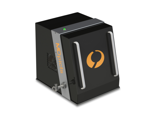
Enables root cause analysis of material defects: destruction free, flexible and precise
Cooling with stirling cooler without handling of liquid nitrogen
Customized laser and optic integration for all your materials
Fully automated temperature dependent measurements
Materials
The MDpicts enables the electrical characterization of almost all semiconductors
Features & Benefits
355–1550 nm
Available wavelengths
10 ns
Time resolution
30–300 K
Temperature range
Repetition
< 60 min.
Measurement time
From the slope of the Arrhenius plot (Fig. 3) the activation energy can be determined.
With the novel commercially available MD-PICTS equipment it is possible to measure the temperature dependence of the photoconductivity transient in a range from 20…500 K. In the past Si, GaAs, InP, SiC and many more semiconductors have already been successfully investigated with this method.
Download
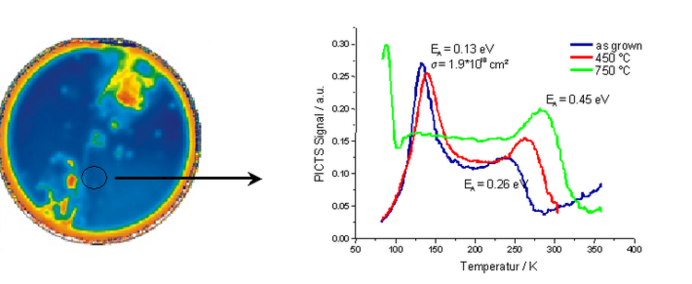
Fig. 4: example of a MD-PICTS spectrum of different tempered Cz—Si wafers
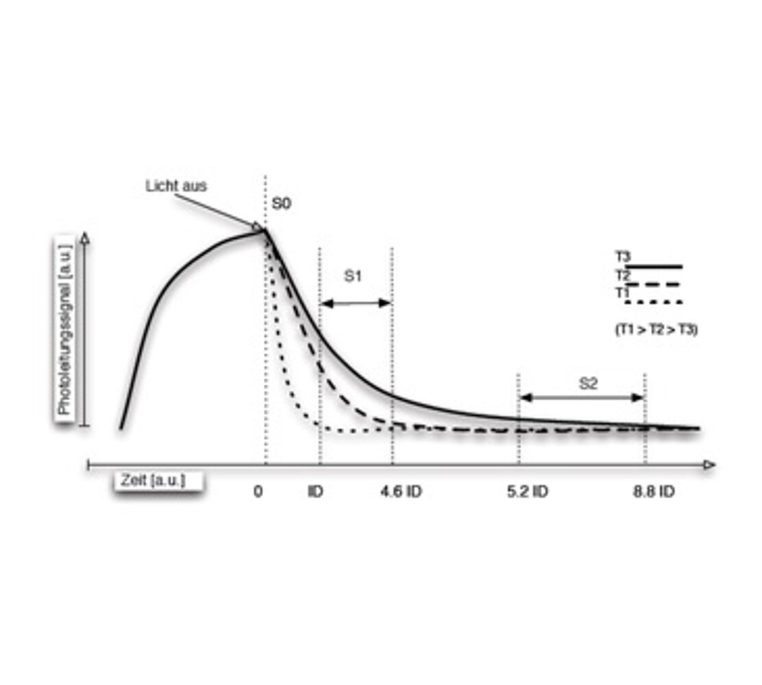
Fig. 1: Temperature dependent carrier emission transients
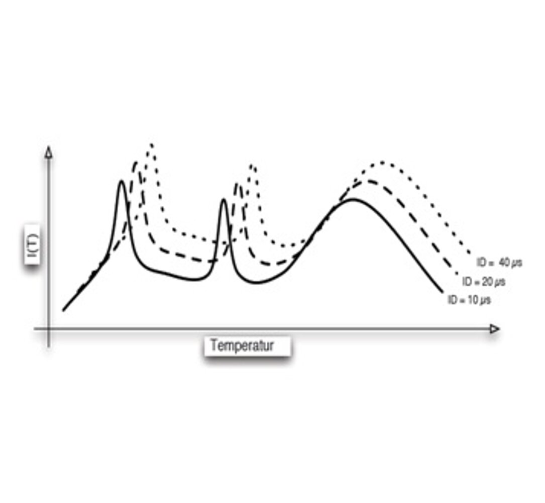
Fig. 2: Box car evaluation with varying ID
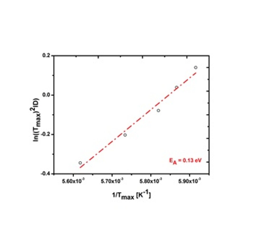
Fig. 3: Arrhenius plot
In order to investigate defects in semiconductors it is widely spread to use temperature dependent methods as deep level transient spectroscopy (DLTS). Usually for these methods it is necessary to form contacts on the samples, which means the sample itself is often altered due to annealing steps. Furthermore for lot of semiconductors some effort is needed to create ohmic contacts at all. MD-PICTS is a non-destructive, contactless method with which the activation energies and capture cross sections of defects can be determined with a high accuracy.
For MD-PICTS measurements the photoconductivity of a sample after the irradiation with light is measured with a resonant microwave cavity. For the determination of the activation energy the temperature dependent change of the photoconductivity transient is determined via a window analysis, which is also used for DLTS measurements (Fig. 1).
Fig.2 shows a so called MD-PICTS spectrum which results from the window analysis. Every peak in this spectrum is a certain defect in the sample.
The temperature shift of the maximum of this peak is plotted in an Arrhenius plot according to this formula of the emission rate:
\(e_{n} = \gamma \sigma_{n}T^2e^{-\frac{E_{A}}{kT}}\)


