Advanced R&D – destruction free, flexible and fast
Highly sensitive due to advanced microwave system
Customized laser and optic integration for all your materials
Simultaneous resistivity measurement and other options
Materials
The MDPmap features a versatile selection of advanced lasers, enabling comprehensive electrical characterization for nearly all types of semiconductors.
Features & Benefits
355–1550 nm
Available wavelengths
10 ns
Time resolution
> 99 %
repeatability
Resistivity
0.3–5
Ohm cm
Flexible mapping tool for R&D or production monitoring
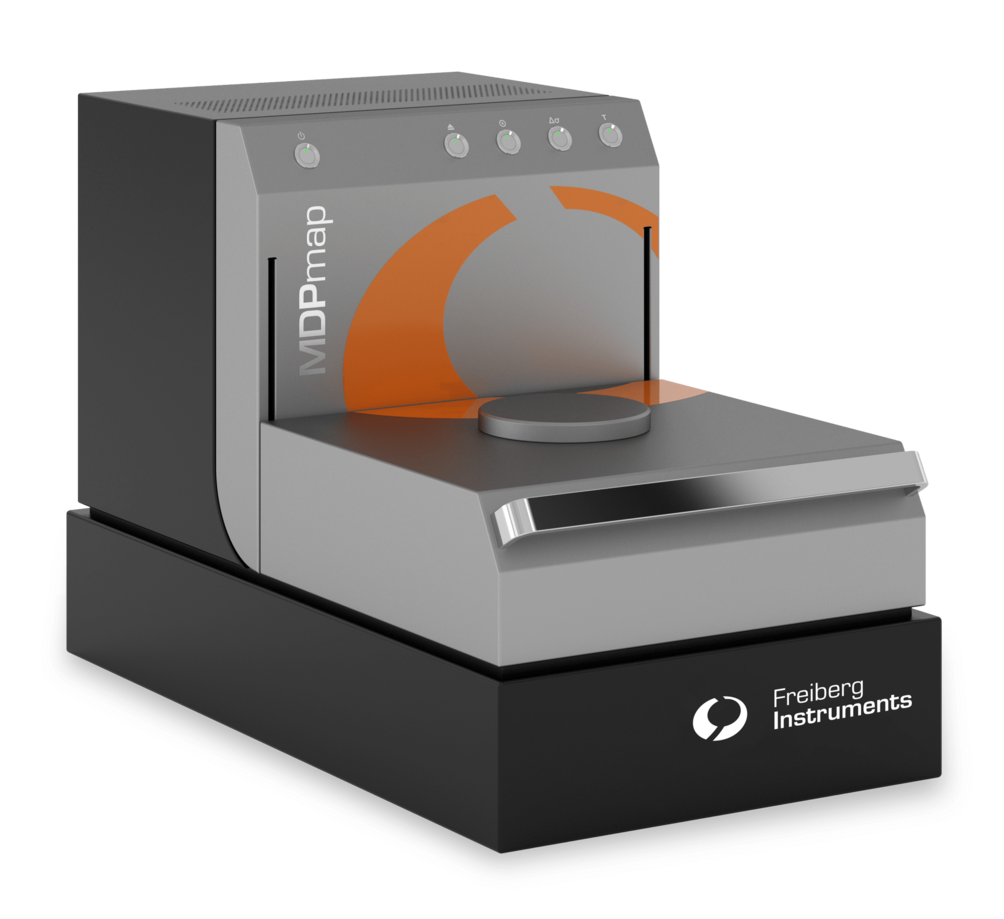
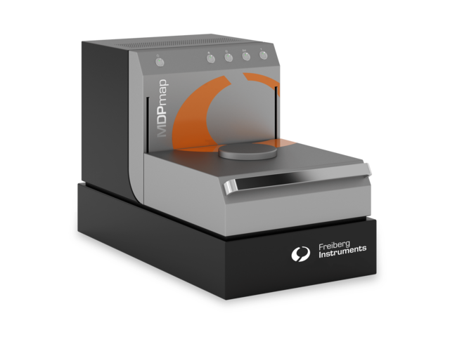
MDPmap is designed as a compact bench top contactless electrical characterization tool for offline production control or R&D, measuring parameters like carrier lifetime, photoconductivity, resistivity and defect information over a wide injection range in steady state or short pulse excitation (μ-PCD). Automated sample recognition and parameter setup allows an easy adaption to a big variety of different samples comprising epitaxial layers and wafers after various preparation stages ranging from as-grown wafers to up to 95% metallized ones.
The major advantage of MDPmap is its high flexibility, which allows for instance the integration of up to four lasers either for injection level dependent lifetime measurements ranging from ultra low to high injection or extracting depth information by using different laser wavelengths. Bias light facility is included as well as options for μ-PCD or steady state injection conditions. A customer defined calculation with different maps is possible as well as an export of primary data for further evaluation. For standard metrology tasks a predefined standard enables routine measurements by only pushing one button.
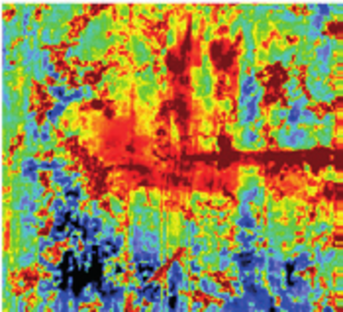
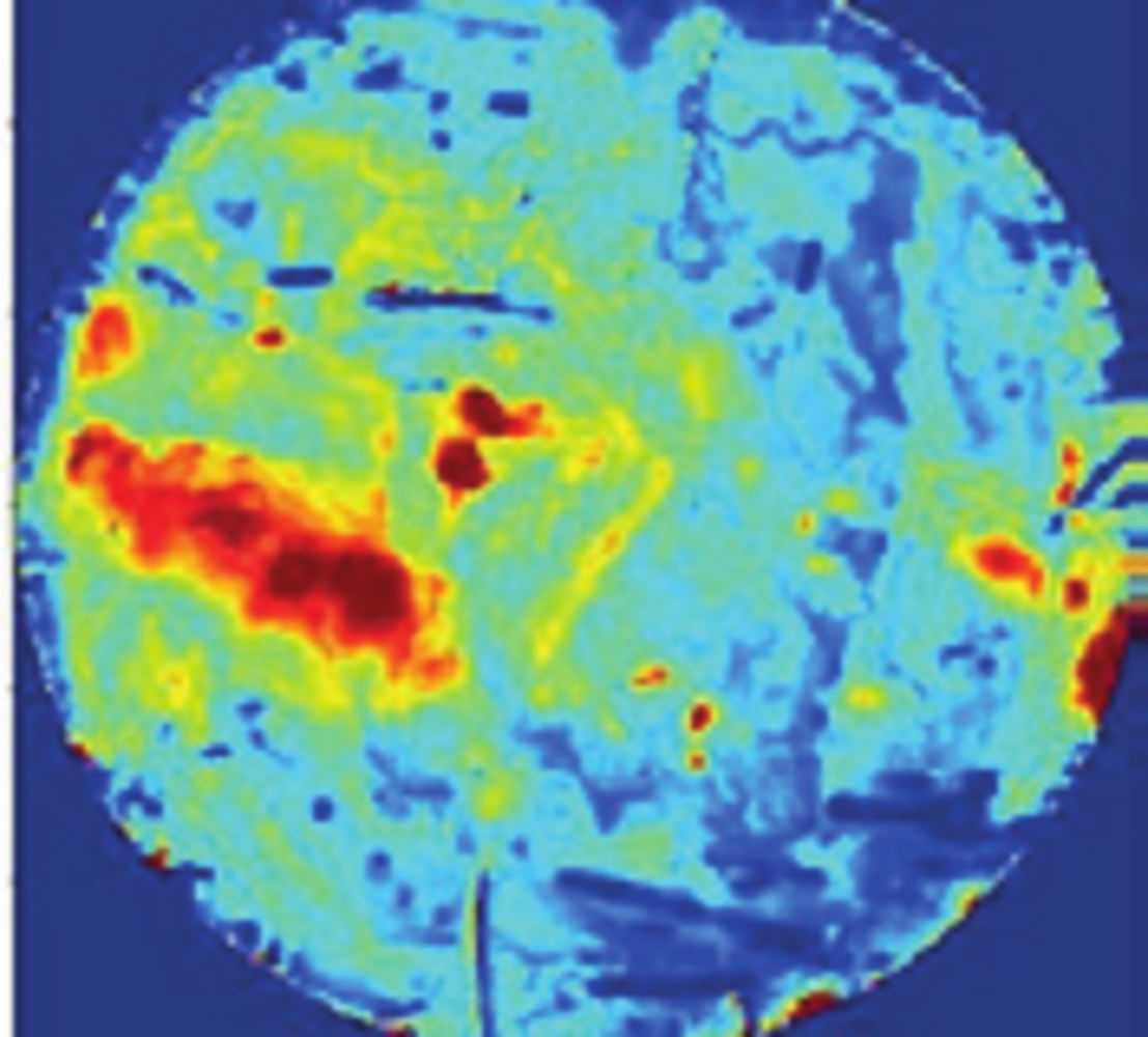
Lifetime map of passivated multicrystalline silicon
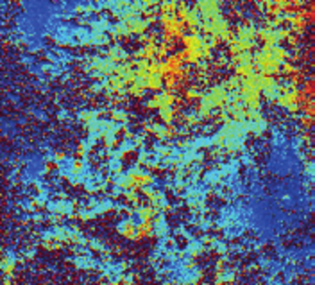
Iron contamination map of multicrystalline silicon
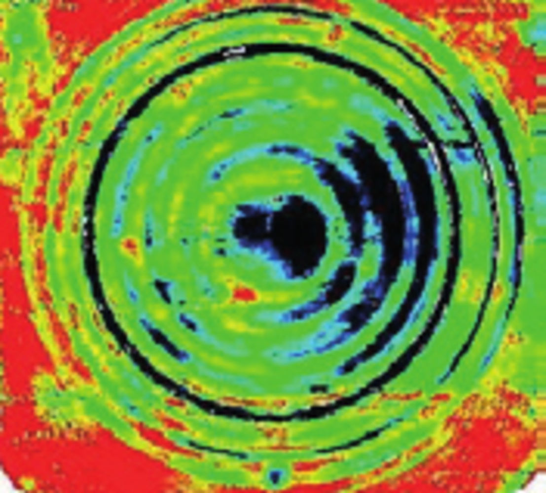
Bor oxygen map of mono silicon
Trap density map of mono silicon
Applications
Technical specifications
| sample size | up to 300 mm diameter (standard), up to 450 mm diameter (on request), down to 5 x 5 mm |
|---|---|
| range of lifetimes | 20 ns to several ms |
| resistivity | 0.2 - >103 Ohm cm, p/n |
| material | silicon wafer, epi layers, partially or fully processed wafers, compound semiconductors and beyond |
| measureable properties | lifetime - μ-PCD/MDP (QSS), photoconductivity |
| excitation | select up to four different wavelengths from 355 nm up to 1480 nm. 980 nm (default) |
| dimensions | 680 x 380 x 450 mm, weight: ca. 65 kg |
| power | 100 - 250V, 50/60 Hz, 5 A |