Found 271 results in 3 milliseconds.

Page

PMT detection unit

Skip breadcrumb navigation Breadcrumb Freiberg Instruments Products Luminescence Dating and Dosimetry lexsygresearch Configuration options PMT detection unit PMT detection unit High-precision detection for groundbreaking analysis results Interested? Get in touch! Contact now Standard UV-VIS PMT unit (300 – 650 nm) Standard UV-VIS PMT unit (280 – 650 nm) standard detection unit for application in luminescence dating and dosimetry bi-alkaline cathode PMT (HAMAMATSU H7360-02) sensitivity range: 300-650 nm peak sensitivity: 420 nm ( 3.1 E5 counts s -1 pW -1 ) dark counts typ. <100 cts photon counter counting linearity (random pulses, 10% loss) 6.0 E6 cps UV-VIS optics Standard UV-VIS PMT unit (280 - 650 nm) Extended UV-VIS PMT unit (160 – 630 nm) for standard applications in luminescence dating and dosimetry detection unit with standard bi-alkaline cathode PMT (Electron Tubes 9235QB) sensitivity 160-630 nm peak sensitivity: 30% quantum efficiency @ 200 nm and 350 nm dark count typ. 300 cts photon counter counting linearity (random pulses, 10% loss) UV-VIS optics Red enhanced UV-VIS PMT unit (300 – 720 nm) Red enhanced UV-VIS PMT unit (300 – 720 nm) necessary/useful if standard UV-VIS PMT sensitivity in the yellow to red wavelength band is insufficient useful e.g. for quartz (flint)/calcite orange-red or feldspar red luminescence measurements thermoelectric/air cooled GaAsP photocathode PMT (HAMAMATSU) sensitivity: 300 – 720 nm peak-sensitivity: 40% quantum efficiency @ 580 nm cooling max. 35 °C below room temperature cooling time approx. 5 min typically 100 cps dark signal at 0°C photon counting system counting linearity (random pulses, 10% count loss) 1.5 E6 cps UV-VIS optics Red enhanced UV-VIS PMT unit (300 - 720 nm) VIS-NIR PMT unit (380 – 890 nm) VIS-NIR PMT unit (380 – 890 nm) required for RF dose determination employing the 865 nm potassium feldspar emission required for 880 nm IRPL detection useful/necessary for any other measurements where red and NIR sensitivity is needed thermoelectric/air cooled GaAs photocathode PMT (HAMAMATSU H7421-50) sensitivity: 380 – 890 nm, peak-sensitivity: 12% quantum efficiency @ 800 nm cooling max. 35 °C below room temperature cooling time approx. 5 min typically 60 cps dark signal at -10°C (125 cps at 0°C) photon counting system counting linearity (random pulses, 10% count loss) 1.5 E6 cps includes UV-NIR optics VIS-NIR PMT unit (380 -890 nm)

Page

PMT detection unit

Skip breadcrumb navigation Breadcrumb Freiberg Instruments Products Luminescence Dating and Dosimetry lexsygsmart Configuration options PMT detection unit PMT detection unit High-precision detection for groundbreaking analysis results Interested? Get in touch! Contact now Standard UV-VIS PMT unit (300 – 650 nm) Standard UV-VIS PMT unit (280 – 650 nm) standard detection unit for application in luminescence dating and dosimetry bi-alkaline cathode PMT (HAMAMATSU H7360-02) sensitivity range: 300-650 nm peak sensitivity: 420 nm ( 3.1 E5 counts s -1 pW -1 ) dark counts typ. <100 cts photon counter counting linearity (random pulses, 10% loss) 6.0 E6 cps UV-VIS optics Standard UV-VIS PMT unit (280 - 650 nm) Extended UV-VIS PMT unit (160 – 630 nm) for standard applications in luminescence dating and dosimetry detection unit with standard bi-alkaline cathode PMT (Electron Tubes 9235QB) sensitivity 160-630 nm peak sensitivity: 30% quantum efficiency @ 200 nm and 350 nm dark count typ. 300 cts photon counter counting linearity (random pulses, 10% loss) UV-VIS optics Red enhanced UV-VIS PMT unit (300 – 720 nm) Red enhanced UV-VIS PMT unit (300 – 720 nm) necessary/useful if standard UV-VIS PMT sensitivity in the yellow to red wavelength band is insufficient useful e.g. for quartz (flint)/calcite orange-red or feldspar red luminescence measurements thermoelectric/air cooled GaAsP photocathode PMT (HAMAMATSU) sensitivity: 300 – 720 nm peak-sensitivity: 40% quantum efficiency @ 580 nm cooling max. 35 °C below room temperature cooling time approx. 5 min typically 100 cps dark signal at 0°C photon counting system counting linearity (random pulses, 10% count loss) 1.5 E6 cps UV-VIS optics Red enhanced UV-VIS PMT unit (300 - 720 nm) VIS-NIR PMT unit (380 – 890 nm) VIS-NIR PMT unit (380 – 890 nm) required for RF dose determination employing the 865 nm potassium feldspar emission required for 880 nm IRPL detection useful/necessary for any other measurements where red and NIR sensitivity is needed thermoelectric/air cooled GaAs photocathode PMT (HAMAMATSU H7421-50) sensitivity: 380 – 890 nm, peak-sensitivity: 12% quantum efficiency @ 800 nm cooling max. 35 °C below room temperature cooling time approx. 5 min typically 60 cps dark signal at -10°C (125 cps at 0°C) photon counting system counting linearity (random pulses, 10% count loss) 1.5 E6 cps includes UV-NIR optics VIS-NIR PMT unit (380 -890 nm)

Product

PSLfood

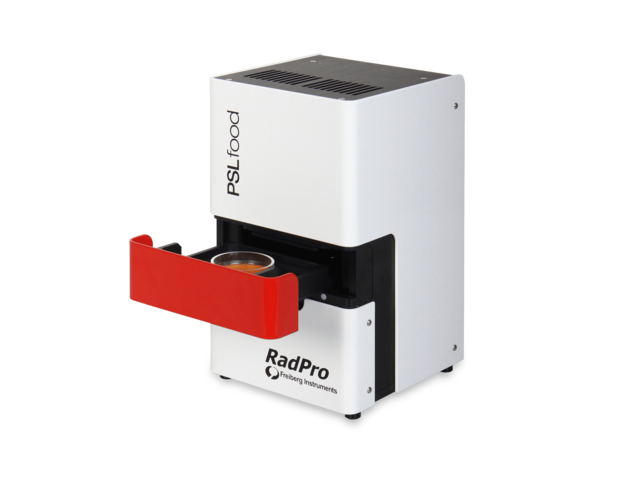
Skip breadcrumb navigation Breadcrumb Freiberg Instruments Products Luminescence Dating and Dosimetry PSLfood PSL food For checking irradiated food according to EN 13751:2009 standard Exclusively through RadPro International Contact for demo Product Sheet Skip menu Quick navigation Features Applications Specifications Contact Features & Benefits PSLfood is a newly developed PSL (OSL) reader for checking irradiated food according to EN 13751:2009 standard (Detection of irradiated food using photo stimulated luminescence). Compact design and newly developed software combines easy operation and excellent performance. Compact and portable The PSLfood drawer is designed for a common petri dish with dimensions of 50 mm in diameter & 20 mm height. The drawer tray and the protection glass can be easily removed for cleaning Applications Food Irradiation Control Food stuff often is irradiated with ionizing radiation for sterilisation purposes. This requires the detection and estimates of the applied doses. The attached mineral dust or the food itself… Learn more PSLfood – Exclusively through RadPro International This product is distributed by our trusted partner. Contact for demo Technical specifications Stimulation IR stimulation with adjustable stimulation power (70 mW/cm² max) Detection unit Photosensor (300-650nm), temperature stabilized, glass protected against sample spill Measurement range 7 decades Stability <1% Detection filter Wide band (standard), IR blocked (BG39), easy to clean Software PSLstudio - User-friendly, designed for routine quality control, different user levels Data output LAN to PC, IP device with worldwide accessibility for remote operation and support Power supply voltage 100-240 V, 50-60 Hz Dimensions approx. 230 mm x 225 mm x 440 mm (L x B x H) Weight 6.5 kg Download Product Sheet PDF (274 KB) PSLfood – Exclusively through RadPro International This product is distributed by our trusted partner. Contact for demo

Page

Peltier cooling

Skip breadcrumb navigation Breadcrumb Freiberg Instruments Products Luminescence Dating and Dosimetry lexsygresearch Configuration options Peltier cooling Peltier cooling for radiation defect characterization Interested? Get in touch! Contact now Low temperature conditions are used for radiation defect characterization. The system is capable of providing stable sample temperatures from -40 °C to -50 °C, while an automated change for high temperature conditions is achieved within seconds, which allows heating up to 710 °C. Min temperature: about -50 °C recommended min temp: -40 °C -40 °C can be kept stable > 60 minutes cooling can be combined with irradiation, OSL, TL, RF, Solar simulation Note: Peltier cooling unit requires vacuum pump and Nitrogen atmosphere

Technology

Penetration depth of different laser wavelength in silicon

Penetration depth of different laser wavelength in silicon In silicon laser light with different wavelength has different penetration depth, hence the right laser should be used for different applications, e.g. for epitaxial layers or investigations of the surface smaller wavelength are ideal. An approximati Penetration depth of different laser wavelength in silicon The microwave detected photoconductivity measures the photoconductivity after the irradiation of the sample with light. Usually the light should have an energy that is higher than the bandgap, so that electrons and holes are created. For silicon this means that a wavelength smaller than 1100 nm should be used. If the surface should be investigated or thin epitaxial layers, it might be useful to use even UV or blue light, which has a much smaller penetration depth in silicon. Figure 1 shows the penetration depth in silicon versus the wavelength and gives the user a hint, which wavelength is most useful for his application. Fig. 1: penetration depth in silicon versus wavelength Matching Products MDP series MDPmap Precision Lifetime Charachterization with Exceptional Sensitivity Learn more MDP series MDPspot Quick and Simple Lifetime Measurement Made Easy Learn more MDP series MDpicts pro High-Resolution, Temperature-Dependent Lifetime Measurement System for Precise Material Characterization Learn more MDP series MDPpro 850+ Advanced Solution for Quality Control of Monocrystalline Silicon Ingots, Bricks, and Wafers Learn more MDP series MDPlinescan Versatile OEM Unit for Lifetime Measurements on Silicon Samples, from Bricks to Processed Wafers Learn more MDP series MDpicts Temperature-Dependent Lifetime Measurement System for Advanced Material Analysis Learn more RES series RESmap High-Precision Resistivity Mapping System for Accurate Material Analysis Learn more Get in touch Do not hesitate to contact us – we are available to assist you with any inquiries or requests. Use our inquiry tool or reach out via email: sales @ freiberginstruments.com

Application

Photo/ Optically Stimulated Luminescence (PSL + OSL)

Photostimulated Luminescence (PSL) Used in wide range of dosimetric applications. Photostimulated Luminescence (PSL or POSL) is also called Optically Simulated Luminescence (OSL) and can be used for a wide range of dosimetric purposes. It is gaining importance in radiation protection dosimetry, personal dosimetry, medical dosimetry and space dosimetry due to the high sensitivity of some phosphors and is a good alternative for film dosimetry. Al 2 O 3 :C from a few µGy up to several Gy BeO from a few µGy up to several Gy Na-dosemeters: Na 2 SiF 6 :Cu,P Other materials like BaSo 4 , BaSo 4 :Eu, … In the form of powder, discs, cubes, … Natural minerals like quartz and feldspar from a few mGy up to several 100 Gy Dating of sediments Higher sensitivity than TL Sensitivity to light requires extra safety precautions Mrozik, A., Bilski, P., Marczewska, B., Obryk, B., Hodyr, K., and Gieszczyk, W. (2014). Radio-photoluminescence of highly irradiated Lif:Mg,Ti and Lif:Mg,Cu,P detectors. Radiation Measurements 71, 31-35. Sądel, M., Bilski, P., and Swakoń, J. (2014). Relative TL and OSL efficiency to protons of various dosimetric materials. Radiation Protection Dosimetry 161, 112-115. Green stimulated OSL response of a single Al2O3:C crystal to 100 cycles of the identical beta dose measured in a lexsyg research Related Solutions and Industries: Luminescence Dating and Dosimetry Matching Products TL/OSL series lexsygsmart The most sensitive TL/OSL reader Learn more TL/OSL series lexsygresearch The most advanced TL/OSL reader Learn more Get in touch Do not hesitate to contact us – we are available to assist you with any inquiries or requests. Use our inquiry tool or reach out via email: sales @ freiberginstruments.com

Technology

Photoconductivity

Photoconductivity When light of sufficient energy is absorbed by a semiconductor, the number of free electrons and holes changes and raises the electrical conductivity of the semiconductor. Photoconductivity When light of sufficient energy is absorbed by a semiconductor, the number of free electrons and holes changes and raises the electrical conductivity of the semiconductor. This increase is called photoconductivity and is dependent of the excess electron and hole concentrations and their mobility via the following equation. [1] \(\Delta\sigma = e \cdot(\mu_{n}\Delta n + \mu_{p} \Delta p)\) [2] \(\Delta\sigma = e \cdot G\) opt \(\cdot \tau \cdot(\mu_{n} + \mu_{p})\) G opt is the optical generation rate, which depends on the incident light intensity, the light spot on the sample and the wavelength. [3] \(G\) opt \(= \alpha \cdot \phi \cdot(1 - R)e^{\alpha x}\) Equation 2 implies that the photoconductivity is proportional to the product of lifetime t and the mobility µ. Therefore, it is also proportional to the square of the diffusion length L, which is defined as: [4] \(L = \sqrt{D \cdot \tau} = \sqrt{\frac{e}{kT} \cdot \mu{\tau}}\) Matching Products MDP series MDpicts pro High-Resolution, Temperature-Dependent Lifetime Measurement System for Precise Material Characterization Learn more MDP series MDPpro 850+ Advanced Solution for Quality Control of Monocrystalline Silicon Ingots, Bricks, and Wafers Learn more MDP series MDPlinescan Versatile OEM Unit for Lifetime Measurements on Silicon Samples, from Bricks to Processed Wafers Learn more MDP series MDpicts Temperature-Dependent Lifetime Measurement System for Advanced Material Analysis Learn more RES series RESmap High-Precision Resistivity Mapping System for Accurate Material Analysis Learn more MDP series MDPmap Precision Lifetime Charachterization with Exceptional Sensitivity Learn more MDP series MDPspot Quick and Simple Lifetime Measurement Made Easy Learn more Get in touch Do not hesitate to contact us – we are available to assist you with any inquiries or requests. Use our inquiry tool or reach out via email: sales @ freiberginstruments.com

Application

Photoconductivity measurements and trap analysis

Photoconductivity measurements and trap analysis of wide bandgap nitride semiconductors Equipped with a 355 nm laser (μ-PCD) or a 375 nm laser diode (MDP), the MDPmap as well as the MDpicts from Freiberg Instruments are suitable for photoconductivity measurements and trap analysis on wide-bandgap nitride semiconductors. The homogeneity of n-type doping can be analyzed by means of the photoconductivity (signal height). It is strongly dependent on the resistivity and the carrier lifetime. The usually long apparent lifetimes are caused by trapping centers in the samples. Deep traps in wide-bandgap semiconductors can be investigated by MDpicts in the temperature range from 30 K up to 800 K. Compared to related methods (e.g. DLTS), MDpicts is a contactless and nondestructive method which also allows the investigation of highly n-doped semiconductors. The trap activation energy can be determined from the slope of the Arrhenius plot or estimated by directly fitting the lifetime reduction as a function of temperature by τ(T)= τ 0 /((1+aexp-E A /kT)). From the value of E A ~ 1.0 eV the main defect in the unintentionally doped GaN sample (see Figure 2 left) can be assumed to be C N . Figure 1: Photoconductivity maps measured by MDP of four different Si doping concentrations in GaN layers. Figure 2: Examples of the MDpicts time constants as a function of inverse temperature for left an unintentionally doped GaN sample and right a Si-doped GaN sample. Related Solutions and Industries: Epitaxial Layers & Thin Films Matching Products MDP series MDpicts Temperature-Dependent Lifetime Measurement System for Advanced Material Analysis Learn more MDP series MDPmap Precision Lifetime Charachterization with Exceptional Sensitivity Learn more Get in touch Do not hesitate to contact us – we are available to assist you with any inquiries or requests. Use our inquiry tool or reach out via email: sales @ freiberginstruments.com

Application

Photoconductivity measurements of implanted samples

Photoconductivity measurements of implanted samples Implantation of B and P are used for many applications in the microelectronic industry, but so far there was no method available to check the homogeneity of these implantations without contacting the samples and (Alttext zu lang) In this case not the lifetime, but the photoconductivity or signal height is the most sensitive parameter for detecting inhomogeneity in implantations. It depends strongly on the resistivity and the lifetime itself. In the MDPmap and MDPingot equipment it is possible to integrate up to 4 lasers with different wavelength. Furthermore it is possible to measure with different pulse length from a very short pulse of only 100 ns, where no carrier diffusion takes place to a pulse length of several ms, where the carriers diffuse into the sample depth. Hence by varying the laser wavelength and the pulse length, it is possible to measure with different penetration. In this case a 660 nm laser with a pulse length of 100 ns was chosen; hence a penetration depth of approximately 4 µs was achieved. Figure 1 shows the implanted P doses in the measured Cz-Si sample and figure 2 demonstrates how the different doses can be distinguished by photoconductivity measurements. Fig. 1: implanted P dosis with a depth of only 2 µm Fig. 2: measured photoconductivity of the sample with different implanted P doses Related Solutions and Industries: Epitaxial Layers & Thin Films Matching Products MDP series MDPmap Precision Lifetime Charachterization with Exceptional Sensitivity Learn more MDP series MDPpro 850+ Advanced Solution for Quality Control of Monocrystalline Silicon Ingots, Bricks, and Wafers Learn more MDP series MDPpro Advanced Lifetime Measurement System for Quality Control and Material R&D on Semiconductors Learn more Get in touch Do not hesitate to contact us – we are available to assist you with any inquiries or requests. Use our inquiry tool or reach out via email: sales @ freiberginstruments.com

Industry

Photovoltaic

Photovoltaic Overcoming Industry Challenges with Cutting-Edge Metrology Solutions Advanced Measurement solutions for maximum yield and efficiency In the last years the overflow of global competitors and a fast-growing global production capacity has led to a dramatically decrease of system prices and put pressure especially on solar cell and module producers. Hence it becomes more and more important to convince customers by a high-quality standard and to further reduce prices. Furthermore, new technologies as TopCon or even Silicon-Perovskite tandem solar cells arise with new challenges for metrology and characterization. Freiberg Instruments metrology solutions are ideal to help increasing the yield and the quality of the produced solar cells as well as characterizing new materials and processes. With them the material quality can be assessed right at the beginning of the production chain and be measured after every production step, from the ingot to the finished solar cell. Key Advantages High measurement speed and sensitivity unsurpassed sensitivity due to our advanced microwave detection system, possibility to measure thin films or solar cells as well as wafers and ingots with a high measurement speed High Accuracy and reproducibility repeatability of below 1% for lifetime measurements and below 3% for resistivity measurements Improvement of material yield Determine the exact cutting criteria for top and bottom of an ingot, incoming inspection of wafers in 1 s Versatile tools for ingots, wafers and even thin films We offer tools for all kinds of different sample geometries from large ingots (up to 850 mm length) to thin films (1 µm thickness and less) Inline metrology for wafers and ingots Lifetime measurements are already a standard method for material quality control in the photovoltaic industry. Taking it one step further, our inline metrology tools allow to sort out low quality parts of the ingot, at as-grown wafers and after every process step. Investigation of surface and bulk quality The separation of bulk and surface quality is one of the main challenges of lifetime measurements. Freiberg Instruments offers a variety of different wavelength with different penetration depth and pulse length as well as estimations for bulk lifetime and surface recombination velocity. Explore our Solutions MDP series Explore more MDPmap Learn more MDPspot Learn more MDPlinescan Learn more MDPpro 850+ Learn more PID series Explore more PIDcon bifacial Learn more SPS/SPV series Explore more HR-SPSmap with fixed energy excitation sources Learn more Expertise in Materials Perovskite Si and more Get in touch Do not hesitate to contact us – we are available to assist you with any inquiries or requests. Use our inquiry tool or reach out via email: sales @ freiberginstruments.com Discover More Solutions Crystal Growth and Processing Learn more Epitaxial Layers & Thin Films Learn more Luminescence Dating and Dosimetry Learn more Research and Development Learn more