Found 271 results in 1 milliseconds.

Page

Red stimulated quartz OSL

Skip breadcrumb navigation Breadcrumb Freiberg Instruments Products Luminescence Dating and Dosimetry lexsygresearch Configuration options Red stimulated quartz OSL Red stimulated quartz OSL allows a separation of the fast OSL component in thermally optically stimulated (TM-OSL) mode Interested? Get in touch! Contact now Following Chruścińska et.al. (2018) and Palczewski & Chruścińska (2019) the stimulation of quartz at 620 nm allows a separation of the fast OSL component in thermally optically stimulated (TM-OSL) mode. Red OSL at 620 nm is now available for lexsyg TL/OSL reader . Chruścińska, A., Szramowski, A., Thermally modulated OSL related to the fast component of the OSL signal in quartz, Radiat. Meas. 120, (2018), 20-25. Palczewski P & Chruścińska A (2019) Different components of the quartz OSL signal resolved by the TM-OSL method. Radiation Measurements 121, 32-36.

Page

Red stimulated quartz OSL

Skip breadcrumb navigation Breadcrumb Freiberg Instruments Products Luminescence Dating and Dosimetry lexsygsmart Configuration options Red stimulated quartz OSL Red stimulated quartz OSL allows a separation of the fast OSL component in thermally optically stimulated (TM-OSL) mode Interested? Get in touch! Contact now Following Chruścińska et.al. (2018) and Palczewski & Chruścińska (2019) the stimulation of quartz at 620 nm allows a separation of the fast OSL component in thermally optically stimulated (TM-OSL) mode. Red OSL at 620 nm is now available for lexsyg TL/OSL reader . Chruścińska, A., Szramowski, A., Thermally modulated OSL related to the fast component of the OSL signal in quartz, Radiat. Meas. 120, (2018), 20-25. Palczewski P & Chruścińska A (2019) Different components of the quartz OSL signal resolved by the TM-OSL method. Radiation Measurements 121, 32-36.

Page

Reference list – TL/OSL reader

Reference list – TL/OSL reader Indian subcontinent Ass.-Prof Dr Manoj Kumar Jaiswal, Department of Earth Sciences, Indian Institute of Science Education and Research, Kolkata, India Dr Manoj K. Rathore, M.P. Council of Science and Technology, Bhopal, India Prof Dr Milap Chand Sharma, Centre for the Study of Regional Development, Jawaharlal Nehru University, New Delhi, India Dr Babita Tiwari, Technical Physics Division (TPD), Bhabha Atomic Research Centre (BARC), Mumabi, India Dr Meghnath Sen, Radiation Safety Systems Division (RSSD), Bhabha Atomic Research Centre (BARC), Mumabi, India Dr Ramanathan Bhavani, TL/OSL Laboratory, Geological Survey of India, Faridabad, India Mr Md. Hossain Khasru and Mr Abdul Baquee Khan Majlis, Geological Survey of Bangladesh, Dhaka, Bangladesh Africa Prof Nabil El-Faramawy, Faculty of Science, Nuclear and Radiation Physics, Ain Shams University, Cairo, Egypt Asia Mr Mohd Sairul Bin Ramle and Mr Ahmad Fadly Bin Jusoh, Pusat Penyelidikan Arkeologi, Universiti Sains Malaysia, Penang, Malaysia Mr En. NorFaizal, Agensi Nuklear Malaysia (Nuklear Malaysia), Kajang Selangor, Malaysia Prof Anchuan Fan, Department History of Science and Scientific Archaeology, University of Science and Technology of China, Hefei, China Ass.-Prof Dr Shibiao Bai, School of Geography Science, Nanjing Normal University, Nanjing, China Dr Weiming Liu, Institute of Hazards and Environment, Chinese Academy of Sciences, Chengdu, China Ms Liu Yang, Institute of Geographical Sciences of Henan Academy of Sciences, Zhengzhou, China Prof Liping Zhou, Department of Geomorphology and Quaternary Geology, College of Urban and Environmental Sciences, Peking University, Beijing, China Prof Xulong Wang and Dr. Shugang Kang, Institute of Earth Environment, Chinese Academy of Sciences, Xi’an, China Ms Wang, Institute of Hydrogeology and Environmental Geology (IHEG), Chinese Academy of Geological Sciences (CAGS), Beijing, China Dr Ma Wei, College of Chemical and Environmental Engineering, Pingdingshan University, Henan, Pingdingshan, China Ms Yang Hui, Institute of Karst Geology, Chinese Academy of Geological Sciences (Karst-CAGS), Guangxi, Guilin, China Dr Toru TAMURA, Marine Geo-Environment Research Group, Research Institute of Geology and Geoinformation, Geological Survey of Japan, National Institute of Advanced Industrial Science and Technology (AIST), Japan Dr Kazumi ITO, Geodynamics Research Group, Research Institute of Earthquake and Volcano Geology, Geological Survey of Japan, National Institute of Advanced Industrial Science and Technology (AIST), Japan Mr Eiji NIKATA, Geophere Science Sector, Civil Engineering, Research Laboratory, Central Research Institute of Electric Power Industry (CRIEPI), Japan Dr Jin Cheul Kim, Surficial Environment & Global Change Department, Korea Institute of Geoscience and Mineral Resources, Korea Mr Jin Myung Kim, Dating Analysis Services Company, Radpion, Korea KFDA (Korean Mininstry of Food and Drug Safety), Gyeongin Regional Office, Korea KFDA (Korean Mininstry of Food and Drug Safety), Seoul Regional Office, Korea Prof Majid Nabi-Bidhendi and Dr Morteza Fattahi, Institute of Geophysics, University of Tehran, Tehran, Iran Prof Dr Mustafa Topaksu, The Faculty of Arts and Sciences, Cukurova University, Adana, Turkey Dr Berna Yildirim, Physical Analysis Laboratory, Tekirdağ Food Control Laboratory Directorate, (Ministry of Food, Agriculture and Livestock), Tekirdağ, Turkey Dr Berrin DİNÇER, Ankara Food Control Laboratory Directorate, Republic of Turkey Ministry of Food Agriculture and Livestock, Ankara, Turkey Dr L.S. Arun Kumar, Medical Physics and Radiation Protection, DGEA, Ministry of Health, Muscat, Sultanate of Oman Prof Leonid Oster, Head of Physics Unit, Shamoon College of Engineering, Israel Dr Chalermpong Polee, Thailand Institute of Nuclear Technology Nuclear Research and Development Division, Nakhon Nayok, Thailand Mr. Weerachat Wiwegwin, Environmental Geology Division, Department of Mineral Resources, Thailand Americas Dr Sebastien Huot, Illinois State Geological Survey, Natural Resources Building, University of Illinois, Champaign, USA Ass.-Prof Luiz G. Jacobsohn, Department of Materials Science and Engineering, COMSET - Center for Optical Materials Science and Engineering Technologies, Clemson University, Anderson, USA Mr Serge Fayeulle, Artemis Testing Lab, Louisville, Colorado, USA Dr Jose Luis Antinao, Indiana Geological Survey, Bloomington, Indiana, USA US Navy, United States of America Dr Shannon Mahan, Geosciences and Environmental Change Science Center, U.S. Geological Survey, Unites States of America Mr Srinivas Sista, GE Healthcare, Wisconsin, United States of America Prof Michel Lamothe, Département des sciences de la Terre et de l'atmosphère, Université du Québec à Montréal, Montréal, Canada Dr Jesus Roman Lopez, Laboratorio de Dosimetria de la Unidad de Irradiacion y Seguridad Radiologica, Instituto de Ciencias Nucleares UNAM, Mexico City, Mexico Dr Helen Jamil Khoury, FACEPE, Recife, Brazil Dr André Oliveira Sawakuchi, Instituto de Geociências, Universidade de São Paulo, São Paulo, Brazil Mr Luiz Carlos Oliveira, University of Sao Paulo, Ribeirao Preto, Brazil Australia and Oceanica Prof Richard (Bert) Roberts, School of Earth and Environmental Science, University of Wollongong, Wollongong, Australia Dr Prabhakar Ramachandran, Princess Alexandra Hospital, Brisbane, Australia Europe Dr Norbert Mercier, Maison de l ' Archéologie, Université Bordeaux Montaigne, Pessac Cedex, France Dr Antoine Zink, Centre de recherche et restauration des musées de France, Palais du Louvre-Porte des Lions, Paris, France Dr Armel Bouvier, Responsable du département archéologie, CIRAM, Martillac, France Ass.-Prof Magali Rizza, CEREGE - OSU Pytheas, Aix-Marseille Université, Marseille, France Dr Emmanuel Vartanian, Re.S.Artes , Bordeaux, France Dr Phillip Toms, School of Natural & Social Sciences, University of Gloucestershire, Cheltenham, United Kingdom Dr Jean-Luc Schwenninger, Research Laboratory for Archaeology and History of Art, University of Oxford, Oxford, United Kingdom Dr Julia Katzmann, Fraunhofer Institute for Ceramic Technologies and Systems IKTS, Dresden, Germany Prof Dr Markus Fuchs, Institut für Geographie, Justus-Liebig-Universität Gießen, Gießen, Germany Dipl.-Geogr. Alexander Fülling, Geographisches Institut, Humboldt-Universität, Berlin, Germany Dr Tobias Lauer, Department of Human Evolution, Max Planck Institute for Evolutionary Anthropology , Leipzig, Germany Dr Clemens Woda, Institute of Radiation Protection, Helmholtz Zentrum München, Munich, Germany Dr Nicole Klasen, Geographisches Institut der Universität zu Köln, Cologne, Germany Dr Christoph Schmidt, Lehrstuhl für Geomorphologie, Universität Bayreuth, Bayreuth, Germany Prof Dr Frank Preusser, Institute of Earth and Environmental Sciences - Geology, University of Freiburg, Freiburg, Germany PD Dr Michael Scholz, GSI Helmholtzzentrum für Schwerionenforschung GmbH, Darmstadt, Germany Dr Sumiko Tsukamoto, Department of Geochronology and Isotope Hydrology, Leibniz Institute for Applied Geophysics, Hannover, Germany Eurofins NDSC Food Testing Germany GmbH, Hamburg, Germany Bundesamt für Strahlenschutz, Oberschleißheim, Germany LMU Klinikum, Munich, Germany Mr Braun, Universitätsklinikum Hamburg-Eppendorf, Hamburg, Germany Labor Kotalla GbR, Haigerloch, Germany Dr Eduardo Gardenali Yukihara, Paul Scherrer Institut, Villigen PSI, Switzerland Dr Jorge Sanjurjo Sánchez, University Institute of Geology, University of A Coruña, Spain Dr Natacha Gribenski, Department of Physical Geography and Quaternary Geology, Stockholm University, Stockholm, Sweden Dr Liliana Stolarczyk, Department of Medical Physics, Institute of Nuclear Physics PAN, Cracow, Poland Prof Dr Eugeniusz Zych, Faculty of Chemistry, University of Wroclaw, Wroclaw, Poland Dr hab. Dariusz Hreniak, Department of Excited State Spectroscopy, Institute of Low Temperature and Structure Research, Polish Academy of Sciences, Wroclaw, Poland Dr Artur Ginter, Thermoluminescence and Spectrometry Laboratory, Institute of Archaeology, University of Lodz, Poland Ms Klaudia Kucińska, National Centre for Radiation Protection in Health Care, Lodz, Poland Prof Dr Andreas Lang and Dr Michael Discher, University of Salzburg, Department of Geography and Geology, Salzburg, Austria Mr Roman Truneček and Ms Veronika Olšovcová, ELI beamlines, Dolní Břežany, Czech Republic Hungarian Academy of Sciences Centre for Energy Research, Radiation Protection Department, Budapest, Hungary Dr Laima Trinkler, University of Latvia, Institute of Solid State Physics, Riga, Latvia
Industry

Research and Development

Research and Development Versatile Measurement solutions to empower and accelerate your R&D progress As a spin-off of the technical university in Freiberg, Freiberg Instruments has a strong scientific background and never stopped cooperating with scientific partners in a variety of research projects to develop measurement tools for the scientific community. Our tools come with a lot of options and accessories to offer tailored solutions to your research needs. Freiberg Instruments even offers customized solutions to ensure top notch research work. Discover R&D Projects Key Advantages Determine exact defect properties Enable temperature dependent measurements in a wide range of temperatures to determine the activation energy of defects High Accuracy and reproducibility High repeatability and reproducibility of all our products as well as reference samples and certificates ensuring traceable to highest standards High measurement speed and sensitivity Unsurpassed sensitivity and measurement speed for crystal orientation as well as lifetime measurements Versatile tools for ingots, wafers and even thin films We offer tools for all kinds of different sample geometries from large ingots (up to 850 mm length) to thin films (1 µm thickness and less) Temperature dependent measurements In order to investigate defects in semiconductors temperature dependent methods are an ideal method to determine activation energies. Usually for these methods it is necessary to form contacts on the samples, which can be very complicated and often alter the samples due to annealing steps. MDpicts is a non-destructive, contactless method with which the activation energies and capture cross sections of defects can be determined with a high accuracy. Investigation of surface and bulk quality The separation of bulk and surface quality is one of the main challenges of lifetime measurements. Freiberg Instruments offers a variety of different wavelength with different penetration depth and pulse length as well as estimations for bulk lifetime. Our Innovative Solutions XRD series Explore more DDCOM Learn more SDCOM Learn more MDP series Explore more MDPmap Learn more MDpicts pro Learn more MDpicts Learn more MDPspot Learn more HTpicts Learn more SPS/SPV series Explore more HR-SPSmap with fixed energy excitation sources Learn more HR-SPSmap with variable energy excitation source Learn more DPM series Explore more DPM100 Learn more Our Partners Get in touch Do not hesitate to contact us – we are available to assist you with any inquiries or requests. Use our inquiry tool or reach out via email: sales @ freiberginstruments.com Discover More Solutions Crystal Growth and Processing Learn more Epitaxial Layers & Thin Films Learn more Photovoltaic Learn more Luminescence Dating and Dosimetry Learn more

Page

Research and Development

Research and Development Driving Innovation Together Advancing Measurement Technology Through Collaboration Research and development (R&D) is at the core of what we do at Freiberg Instruments. We partner with industry leaders, universities, and research institutions to push the boundaries of measurement technology and develop cutting-edge solutions. Contact Us Our Research and Development Services We collaborate closely with our partners to drive innovation in precision measurement. Our services include: New Technology Development Pioneering measurement techniques that enhance accuracy, speed, and efficiency for industrial and research applications. Prototyping & Testing Developing, refining, and testing new instruments to meet emerging challenges in high-tech industries. Customized Research Solutions Tailored R&D projects designed to address specific measurement challenges and application needs. Collaboration with Universities & Industry Joint research initiatives that bridge the gap between academic discoveries and industrial applications. Our Process: From Idea to Innovation Identifying Research Needs: We work with customers and partners to define key research objectives and technical challenges. Concept & Feasibility Study: Our experts assess potential solutions, conduct feasibility studies, and outline the development roadmap. Development & Prototyping: We design, build, and test new measurement technologies to validate their performance. Implementation & Optimization: Once validated, we integrate innovations into practical applications, refining them for real-world use. Why Choose Freiberg Instruments for R&D? Innovative Spirit A strong commitment to advancing measurement technology through continuous research. Collaborative Approach Close partnerships with academia and industry to create impactful solutions. Cutting-Edge Expertise A team of specialists dedicated to pushing the limits of precision measurement. Proven Track Record Years of successful R&D projects leading to groundbreaking advancements. Our Partners Innovation drives progress. Started as a university spin-off, we turn new ideas into high-performance measurement solutions through research and collaboration that shape the future. Dr. Nadine Schüler Head of Research & Development Let’s Shape the Future of Measurement Technology Interested in partnering with us on a research project? Contact us to explore collaboration opportunities in advancing measurement solutions. Use our inquiry tool or reach out via email: sales @ freiberginstruments.com Discover more Customization Learn more Automation Learn more Training and Application Expertise Learn more Technical Support Learn more

Application

Resistance measurements on wafers and bricks

Resistance measurements on wafers and bricks The resistivity is one of the most important electrical parameters of a material. It is a key parameter for the performance of semiconductor devices as e.g. solar cells and depends on the doping density of the material. (Alttext Kürzen) With MDPmap and MDPingot it is possible to measure the resistivity of wafers or bricks with a high accuracy and a resolution of 1 mm via eddy current measurements. The Eddy current sensor setup has a very good long-term stability, due to a distance correlated internal calibration matrix. Hence, with every resistivity map a geometry map of the surface flatness is measured. The resistivity can be measured simultaneously with the minority carrier lifetime and photoconductivity maps. In case of wafer measurements, the thickness of the sample has to be given by the user. Step width ≥ 1mm Edge exclusion 12 mm Resistivity wafer thickness range 150 ...250 µm Resistivity range can be specified Default setting: 0.5 to 5 Ohm cm Accuracy: < 5 % Repeatability: < 1 % (range of 0.5 until 3 Ohm cm) It is possible to map the sheet resistance of the emitter, in order to investigate the homogeneity of the emitter diffusion. The resistivity of the base has to be given by the user. Sheet resistance measurement with range 0.1-200 Ohm/sq Accuracy at standard sample size, 0.1 - 10 Ohm/sq: < 3 % accuracy 10 - 100 Ohm/sq: < 4 % accuracy 100 – 200 Ohm/sq: < 5 % accuracy Figure 1 to 3 show examples of resistivity maps measured on mc-Si wafers and bricks. Fig 1: Emitter sheet resistance map of a typical mc-Si wafer with emitter diffusion and an average sheet resistance of 85.1 Ohm/sq. Fig. 2: resistivity map of a typical mc-Si wafer for PV applications and an average resistivity of 1.0 Ohm cm Fig. 3: Resistivity map of a typical mc-Si brick for PV applications and an average resistivity of 1.4 Ohm cm Related Solutions and Industries: Epitaxial Layers & Thin Films , Photovoltaic Matching Products MDP series MDPspot Quick and Simple Lifetime Measurement Made Easy Learn more MDP series MDPpro 850+ Advanced Solution for Quality Control of Monocrystalline Silicon Ingots, Bricks, and Wafers Learn more MDP series MDPpro Advanced Lifetime Measurement System for Quality Control and Material R&D on Semiconductors Learn more MDP series MDPmap Precision Lifetime Charachterization with Exceptional Sensitivity Learn more Get in touch Do not hesitate to contact us – we are available to assist you with any inquiries or requests. Use our inquiry tool or reach out via email: sales @ freiberginstruments.com

Technology

Resistivity

Resistivity measurement and mapping Resistivity mapping and measurement The electrical resistivity directly depends on the density of the semiconductor and is therefore a useful parameter to monitor doping profiles and homogeneity. The lifetime and diffusion length depend on the doping density as well. Since doping shifts the fermi level, it increases the rate of SRH recombination in most cases. In addition, since Auger recombination is more likely in heavily doped material, the recombination process itself is enhanced as the doping increases. In our systems the resistivity is measured via the non-contact eddy current method. Eddy current is caused when a sample is exposed to a changing magnetic field due to variations of the field with time, for example if an AC current flows in a coil in close proximity to the sample. This causes a current within the bulk of the sample and the circulating eddies of current create induced magnetic fields that oppose the change of the original magnetic field. The greater the electrical conductivity of the sample , the greater are the currents that are developed and the greater the opposing field will be. In other words the electrical loss in the material is measured, which is directly related to the resistivity of the sample. Note that the measurement depends also on the distance from the coil to the sample and therefore on geometrical features of the sample. Resistance measurements on wafers and bricks The resistivity is one of the most important electrical parameters of a material. It is a key parameter for the performance of semiconductor devices as e.g. solar cells and depends on the doping density of the material. Hence, it is necessary to measure the resistivity with a high accuracy and a high resolution, in order to detect inhomogeneity in the doping density. Read more Matching Products MDP series MDpicts pro High-Resolution, Temperature-Dependent Lifetime Measurement System for Precise Material Characterization Learn more MDP series MDPpro 850+ Advanced Solution for Quality Control of Monocrystalline Silicon Ingots, Bricks, and Wafers Learn more MDP series MDPlinescan Versatile OEM Unit for Lifetime Measurements on Silicon Samples, from Bricks to Processed Wafers Learn more MDP series MDpicts Temperature-Dependent Lifetime Measurement System for Advanced Material Analysis Learn more RES series RESmap High-Precision Resistivity Mapping System for Accurate Material Analysis Learn more MDP series MDPmap Precision Lifetime Charachterization with Exceptional Sensitivity Learn more MDP series MDPspot Quick and Simple Lifetime Measurement Made Easy Learn more Get in touch Do not hesitate to contact us – we are available to assist you with any inquiries or requests. Use our inquiry tool or reach out via email: sales @ freiberginstruments.com

Page

Resistivity Mapping

Resistivity Mapping Accurate Material Analysis for Semiconductor Quality Control: The RES series Advanced resistivity mapping is essential for semiconductor quality control across materials like SiC, GaN, InP, and more. Using eddy-current sensing, it enables non-contact, high-precision measurements with excellent repeatability (σ < 0.15%), even on complex shapes such as wafers, boules, and ingots. Integrated distance and temperature sensors ensure stable, accurate results by compensating for external and material-related variations. Automation in resistivity mapping has significantly increased throughput and reduced manual intervention. With X-Y mapping capabilities and multi-point measurement resolution as fine as ±0.1 mm, these systems are optimized for both research labs and high-volume manufacturing. Easy calibrating routines and compatibility with industry standards like SEMI MF 673 help streamline setup and maintain long-term system performance. Combining high sensitivity, automation, and broad material compatibility, this technology supports a wide range of semiconductor applications—helping manufacturers improve yield, accelerate development, and scale with confidence. RES series RESmap Learn more The market launch of RESmap was a special milestone – a game changer for the semiconductor industry. Dr. Christian Hagendorf Key Account Manager Get in touch Do not hesitate to contact us – we are available to assist you with any inquiries or requests. Use our inquiry tool or reach out via email: sales @ freiberginstruments.com

Product

SDCOM

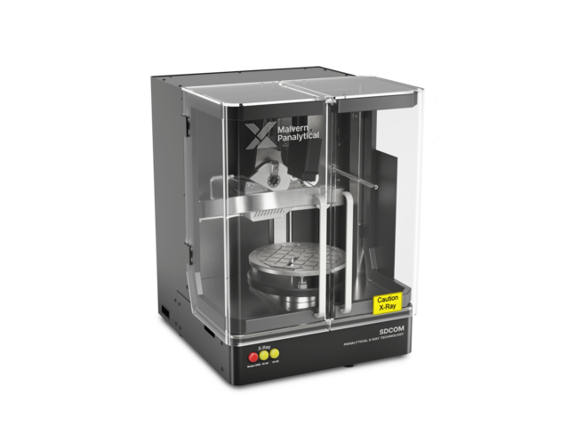
Skip breadcrumb navigation Breadcrumb Freiberg Instruments Products X-ray Diffraction SDCOM SDCOM Ultra-fast, top surface measuring crystal orientation in a compact package Exclusively through Malvern Panalytical Contact for demo Product Sheet Skip menu Quick navigation Features Applications Technology Software Contact Materials With SDCOM, a wide variety of materials can be precisely analyzed. Thanks to their flexibility and performance, our systems meet even the most demanding requirements. Ag Al₂O₃ (sapphire) AlSb Au CdTe GaAs GaN GaP GaPO₄ GaSb Ge InAs InP InSb La₃Ga₅SiO₁₄ LaTiO₃ LiF LiNbO₃ Mg₂SiO₄ MgAl₂O₄ MgF₂ MgO NdGaO₃ Ni PbS PbTe Pt Si SiC 2H SiC 4H SiC 6H SiC 15R SiC₃C SiO₂ (quartz) SnTe SrLaAlO₄ SrTiO₃ TiO₂ ZnO ZnTe and more Features & Benefits Ability to measure very small crystals down to 1 mm or larger samples Variety of sample holders and transfer fixtures towards wire saw, grinding, etc. Marking option of lateral crystal direction No water cooling Highest precision: 0.01° (depending on crystal quality) Determination of the complete lattice orientation of single crystals Ultra-fast crystal orientation measurement using the Omega-scan method Air cooled X-ray tube, no water cooling required Appropriate for research and production quality control manual handling (no automation option) Crystal orientation is determined by reflex position suitable for a vast variety of materials Applications Samples with a wide variety of geometry & size The industrial synthesis of single crystals begins with large, heavy boules and is processed down to smaller forms, such as wafers or blanks. In experimental growth, tiny cylinders are produced.… Learn more Marking and measuring of in-plane directions The Omega Scan provides a complete crystal orientation in a single measurement, allowing for the direct identification of in-plane directions. This feature is particularly useful for marking… Learn more Crystal quality Crystal quality cannot be directly measured, but several physical properties can be assessed and compared to standards for pure, homogeneous crystals. One such property is the half-width of an… Learn more NLO Materials: Crystal Quality & Optical Axis Orientation Unlike typical inorganic metals, semiconductors, and insulators, NLO materials feature more complex crystal structures with lower symmetry. This structure creates a highly anisotropic environment… Learn more SDCOM – Exclusively through Malvern Panalytical This product is distributed by our trusted partner. Contact for demo Technologies Omega-scan Ultra-Fast Orientation Measurement for Single Crystals Learn more Theta-scan Precision X-ray Method for Single Crystal Orientation Learn more Software XRDStudio Multiple Operating ModesOperator Mode: Designed for fixed measurement parameters, ensuring a safe and streamlined workflow. Administrator Mode: Allows for the creation and modification of… Learn more SDCOM – Exclusively through Malvern Panalytical This product is distributed by our trusted partner. Contact for demo

Technology

SPV signal analysis: fits and simulations

SPV signal analysis: fits and simulations Charge dynamic simulations in photoactive materials, incl. heterojunction photoactive materials. We are currently developing simulation tools to enable first principle calculations of the electronic structure in a given photoactive material or material combination, based on solid-state physics. The SPS/SPV simulation tool enables users of any SPS/SPV equipment to verify their measurements against simulated scenarios. Thereby for instance reducing development time for new materials research and/or testing the tolerances of a given photoactive material configuration. All transient responses can be fitted between 10 ns and 100 ms using the build-in stretched exponentials multi-parameter fit function with three basic parameters; t I , β i and A i , where t is the transient time constant, β is the stretching factor to the exponential function and A is the signal amplitude. The multi-parameter i can in most cases be limited to 2 (i.e. i = 1,2), 5 is rare, but sometime needed for complex structures. In principle, fitting with i = 1,….,12 is possible. Figure 1 shows an example using SPV for the radial characterization of shallow defects close to the conduction band in a float zone silicon wafer using a fit function consisting of the sum of 5 stretched exponential functions. Matching Products SPS/SPV series HR-SPSmap with fixed energy excitation sources High-Resolution and Sensitive Surface Photovoltage Measurement Solutions Learn more SPS/SPV series HR-SPSmap with variable energy excitation source with a variable energy excitation source Learn more DPM series DPM100 Wide range double prism monochromator Learn more Get in touch Do not hesitate to contact us – we are available to assist you with any inquiries or requests. Use our inquiry tool or reach out via email: sales @ freiberginstruments.com