Found 271 results in 2 milliseconds.

Product

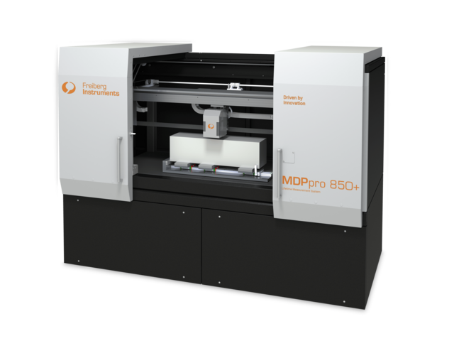
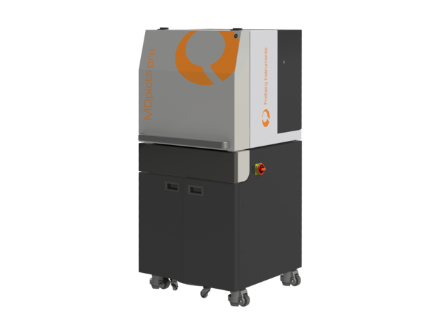
MDPpro 850+

Skip breadcrumb navigation Breadcrumb Freiberg Instruments Products Microwave Detected Photoconductivity MDPpro 850+ MDPpro 850+ Advanced Solution for Quality Control of Monocrystalline Silicon Ingots, Bricks, and Wafers Interested? Get in touch! Contact now Product Sheet Skip menu Quick navigation Features Applications Specifications Technology Options Software Contact Materials For HJT, HIT, TOPcon, bifacial PERC, PERC+ solar cells and more. Si Perovskite and more Features & Benefits Range of lifetimes: 20 ns to 100 ms (for samples > 0.3 Ohm cm) SEMI standard: PV9-1110 Measurement speed: < 30 sec for linescan < 5 min for complete mapping Simultaneous measurement of: lifetime μPCD/MDP (QSS) and resistivity Automatic geometric recognition: G12, M10 bricks and wafers Slip lines in Cz-Si ingot Lifetime measurement of a quasi-mono Si ingot with a lot defects Applications Resistance measurements on wafers and bricks With MDPmap and MDPingot it is possible to measure the resistivity of wafers or bricks with a high accuracy and a resolution of 1 mm via eddy current measurements. The Eddy current sensor setup… Learn more Light Beam Induced Current (LBIC) The proceeding is based on the measurement of the local short circuit current Isc in the cell, which is produced through appropriate excitation. For the measurement the solar cell is contacted… Learn more Iron concentration determination With the MDPingot and MDPmap series it is possible to measure the iron concentration in bricks and wafers fully automated and with a very high resolution. Lifetime measurements before and after… Learn more p/n detection in bricks In the PV industry sometimes also low quality material with a high phosphorous concentration is used. Phosphor has a segregation coefficient of 0.35 and is therefore segregating in the top of the… Learn more Detection of CrB in silicon Lifetime measurements before and after chromium boron pair dissociation is a widely used method for chromium determination in silicon wafers. In boron doped silicon with a high doping… Learn more Detection of BO2 in silicon The boron-oxygen complexes can be activated by irradiating the sample with light and deactivated by heating the sample at 200 °C for several minutes. This can be used similar to the iron… Learn more Trap concentration determination With the MDPmap and MDPingot it is possible to measure the photoconductivity as well as the minority carrier lifetime with one measurement and fully automated in a wide injection range. A clever… Learn more Injection dependent measurements With MDPmap it is possible to measure not only injection dependent lifetime curves but also photoconductivity curves over a very wide range of injection. In the MDPmap and MDPingot up to 4… Learn more Inline metrology of mc-Si bricks With the MDPinline ingot it is possible to measure all 4 sides of a brick in under 1 min per side with 1 mm resolution. At the same time a spatial resolved measurement of conduction type changes… Learn more Photoconductivity measurements of implanted samples In this case not the lifetime, but the photoconductivity or signal height is the most sensitive parameter for detecting inhomogeneity in implantations. It depends strongly on the resistivity and… Learn more Lifetime determination of epitaxial silicon thin-film layers With MDP it is possible to measure the lifetime of minority carriers and the photoconductivity in epitaxial layers as fast and exactly as possible with a high resolution. The measurement of… Learn more Interested? Our experts are happy to assist you. Get in touch! Contact us now! Technical specifications Material monocrystalline silicon Ingot size between 125 x 125 to 210 x 210 mm², brick length 850 mm or longer Wafer Size up to 300 ¬mm diameter Resistivity range 0.5 – 5 Ohm cm. Other ranges on request Conduction type p, n Measurable properties lifetime - μPCD/MDP (QSS), photoconductivity, resistivity and more Default excitation lR laser diode (980 nm, max. 500 mW) and IR laser diode (905 nm, max. 9000 mW). Other wavelengths are available on request PC workstation Windows 11 or latest, .NET Framework update, 2 Ethernet ports Power requirements 100 – 250 V AC, 6 A Dimensions (W × H × D) 2560 × 1910 × 1440 mm Weight approx. 200 kg Certification manufactured under ISO 9001 guidelines, CE conform Download Product Sheet PDF (361 KB) Technologies Minority carrier lifetime The measured effective lifetime is composed of the bulk lifetime and surface lifetime, which depends on the surface properties of a sample. Hence the surface has to be passivated, if you want… Learn more Photoconductivity When light of sufficient energy is absorbed by a semiconductor, the number of free electrons and holes changes and raises the electrical conductivity of the semiconductor. This increase is… Learn more Resistivity The electrical resistivity directly depends on the density of the semiconductor and is therefore a useful parameter to monitor doping profiles and homogeneity. The lifetime and diffusion length… Learn more Mobility The mobility is a quantity related to the drift velocity of electrons or holes in an applied electric field across a material. The mobility depends on different scattering processes that can… Learn more Diffusion length Learn more Defect properties The properties of a defect and its impact on the material quality can be described by three main parameters:defect concentration NT, capture cross sections for electrons and holes σn, σp,… Learn more Lifetime simulations From the simulated time dependent carrier concentrations the photoconductivity can be calculated using the mobility model of DORKEL and LETURCQ [2] . The minority carrier lifetime can be… Learn more Simulation of carrier profiles The measurement of thick samples as bricks leads to new questions and problems. One of these questions is how the carrier profiles that develops in a sample effect the lifetime measurements. To… Learn more Microwave detected photoconductivity (MDP) The novel method MDP is well suited for both, defect investigation by e.g. injection dependent minority carrier lifetime measurements, as well as mapping of wafers or even bricks for inline… Learn more Comparison to µ-PCD and QSSPC Besides MDP the two most important contact less lifetime measuring methods are QSSPC (quasi steady state photoconductivity) and µ-PCD (microwave detected photoconductive decay). Currently one… Learn more MD-PICTS MD-PICTS is a modification of MDP, where temperature dependent measurements of the defect part of the transient are accomplished. This allows for a spatially resolved defect characterization.… Learn more Penetration depth of different laser wavelength in silicon The microwave detected photoconductivity measures the photoconductivity after the irradiation of the sample with light. Usually the light should have an energy that is higher than the bandgap,… Learn more Materials Electrical properties and defects of a large variety of semiconductor materials, devices and dielectric materials can be investigated contact less and destruction with our advanced method MDP.… Learn more Accessories & Options Our devices offer versatile configuration options to meet specific requirements effectively. Each model can be customized to ensure maximum flexibility and efficiency. Contact for more information Spot size variation Resistivity measurement (bricks/wafers) Background/Bias light Refl ection measurement (MDP) LBIC Internal iron mapping of p-doped Si P/N detection Bar code reader Automatic geometric recognition Wide range of lasers Software XRDStudio Multiple Operating ModesOperator Mode: Designed for fixed measurement parameters, ensuring a safe and streamlined workflow. Administrator Mode: Allows for the creation and modification of… Learn more Get in touch Do not hesitate to contact us – we are available to assist you with any inquiries or requests. Use our inquiry tool or reach out via email: sales @ freiberginstruments.com
Product

MDpicts pro

Skip breadcrumb navigation Breadcrumb Freiberg Instruments Products Microwave Detected Photoconductivity MDpicts pro MDpicts pro High-Resolution, Temperature-Dependent Lifetime Measurement System for Precise Material Characterization Interested? Get in touch! Contact now Product Sheet Laser Selection Guide Skip menu Quick navigation Features Applications Specifications Technology Contact Enables root cause analysis of material defects: destruction free, flexible and precise High spatial resolution Customized laser and optic integration for all your materials Novel cryostat for samples up to 4’’ Materials The MDpicts pro enables the electrical characterization of almost all semiconductors Si SiC Ge GaAs Ga₂O₃ InP Diamond and more Features & Benefits 355–1550 nm Available wavelengths 10 ns Time resolution 83–300 K Temperature range 10 µm Spatial resolution 10 µm Spatial resolution Applications Light Beam Induced Current (LBIC) The proceeding is based on the measurement of the local short circuit current Isc in the cell, which is produced through appropriate excitation. For the measurement the solar cell is contacted… Learn more Microwave Detected Photo Induced Current Transient Spectroscopy In order to investigate defects in semiconductors it is widely spread to use temperature dependent methods as deep level transient spectroscopy (DLTS). Usually for these methods it is necessary… Learn more Investigation of defect levels in InP MD-PICTS is a well suited method for the investigation of defect levels in InP. For example investigations on indium phosphide shows that the defect content changes during annealing processes,… Learn more Interested? Our experts are happy to assist you. Get in touch! Contact us now! Technical specifications temperature range 83 – 350 K sample size up to 4" wafers small wafer pieces resistivity 0.2 - >10 10 Ωcm conduction type p,n minority carrier lifetime 20 ns – 100 ms measurable properties lifetime, photoconductivity, activation energy, etc. excitation 355 – 1550 nm Technologies Minority carrier lifetime The measured effective lifetime is composed of the bulk lifetime and surface lifetime, which depends on the surface properties of a sample. Hence the surface has to be passivated, if you want… Learn more Photoconductivity When light of sufficient energy is absorbed by a semiconductor, the number of free electrons and holes changes and raises the electrical conductivity of the semiconductor. This increase is… Learn more Resistivity The electrical resistivity directly depends on the density of the semiconductor and is therefore a useful parameter to monitor doping profiles and homogeneity. The lifetime and diffusion length… Learn more Mobility The mobility is a quantity related to the drift velocity of electrons or holes in an applied electric field across a material. The mobility depends on different scattering processes that can… Learn more Diffusion length Learn more Defect properties The properties of a defect and its impact on the material quality can be described by three main parameters:defect concentration NT, capture cross sections for electrons and holes σn, σp,… Learn more Lifetime simulations From the simulated time dependent carrier concentrations the photoconductivity can be calculated using the mobility model of DORKEL and LETURCQ [2] . The minority carrier lifetime can be… Learn more Simulation of carrier profiles The measurement of thick samples as bricks leads to new questions and problems. One of these questions is how the carrier profiles that develops in a sample effect the lifetime measurements. To… Learn more Microwave detected photoconductivity (MDP) The novel method MDP is well suited for both, defect investigation by e.g. injection dependent minority carrier lifetime measurements, as well as mapping of wafers or even bricks for inline… Learn more Comparison to µ-PCD and QSSPC Besides MDP the two most important contact less lifetime measuring methods are QSSPC (quasi steady state photoconductivity) and µ-PCD (microwave detected photoconductive decay). Currently one… Learn more MD-PICTS MD-PICTS is a modification of MDP, where temperature dependent measurements of the defect part of the transient are accomplished. This allows for a spatially resolved defect characterization.… Learn more Penetration depth of different laser wavelength in silicon The microwave detected photoconductivity measures the photoconductivity after the irradiation of the sample with light. Usually the light should have an energy that is higher than the bandgap,… Learn more Materials Electrical properties and defects of a large variety of semiconductor materials, devices and dielectric materials can be investigated contact less and destruction with our advanced method MDP.… Learn more Get in touch Do not hesitate to contact us – we are available to assist you with any inquiries or requests. Use our inquiry tool or reach out via email: sales @ freiberginstruments.com
Product

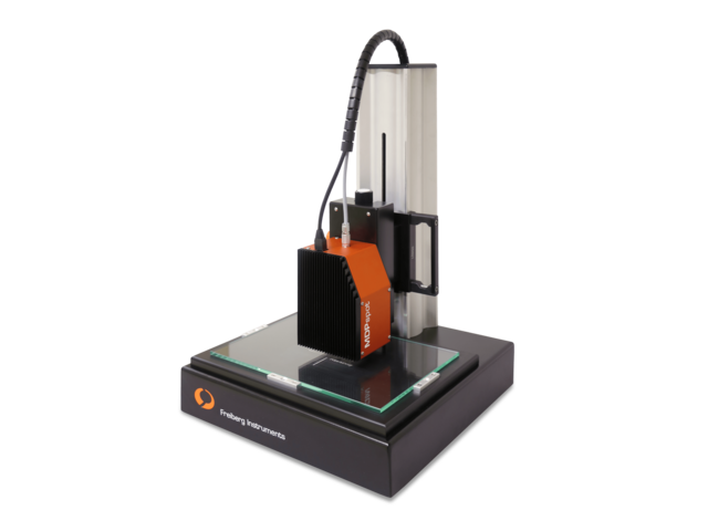
MDPspot

Skip breadcrumb navigation Breadcrumb Freiberg Instruments Products Microwave Detected Photoconductivity MDPspot MDPspot Quick and Simple Lifetime Measurement Made Easy Interested? Get in touch! Contact now Product Sheet Laser Selection Guide Skip menu Quick navigation Features Applications Specifications Technology Options Contact Enables fast and easy assessment of the lifetime at a single point Single point measurement Wafers and ingots Flexible low cost tool Materials Discover unparalleled ease and speed in lifetime characterization of almost all semiconductors with MDPspot, designed to streamline your workflow without compromising accuracy. Si SiC Ge GaN GaAs InP and more Features & Benefits 355–1550 nm Available wavelengths 10 ns Time resolution > 99 % repeatability Flexible measurement For wafers and ingots Flexible measurement For wafers and ingots contactless destruction free electrical semiconductor characterisation μ-PCD measurement option included advanced sensitivity for visualisation of so far invisible defects and investigations of epitaxial layers integration of up to four lasers for a wide range of injection levels access to primary data of single transients as well as maps for special evaluation purposes allows for single wafer investigation different recipes for different wafer classes monitoring of material, process quality and stability Table top single spot measurements The MDPspot is an affordable and compact solution for lifetime characterization of various semiconductors across different preparation stages. Designed without built-in automation, it offers flexibility for diverse applications. Cost-Effective Design : A budget-friendly option for reliable lifetime measurements. Versatile Compatibility : Suitable for a range of semiconductors samples, from thin wafers to thicker materials up to 156 mm bricks. Optional Z-Axis Adjustment : A hand-operated z-axis is available for precise handling of thicker samples. Intuitive Software : Standard software included for clear visualization and analysis of results. Streamline your measurement processes with this efficient and easy-to-use system. Applications Resistance measurements on wafers and bricks With MDPmap and MDPingot it is possible to measure the resistivity of wafers or bricks with a high accuracy and a resolution of 1 mm via eddy current measurements. The Eddy current sensor setup… Learn more Minority carrier lifetime measurements on SiC In recent years the quality of SiC materials has improved profoundly and hence SiC is becoming more and more a competitor to Si for e.g. high-power devices. Since it is a wide-bandgap… Learn more Investigation of material quality of GaAs In contrast to other techniques MD-PICTS (microwave detected photo induced current transient spectroscopy) can detect signals even from thin surface regions (3 µm) of SI GaAs samples and is… Learn more Injection dependent measurements With MDPmap it is possible to measure not only injection dependent lifetime curves but also photoconductivity curves over a very wide range of injection. In the MDPmap and MDPingot up to 4… Learn more Highly spatial resolved inline metrology on Multicrystalline Silicon Non-destructive measurements of minority carrier lifetime are well established and widely used for process control and characterization of defects in crystalline silicon. With our tool MDPinline… Learn more Determination of passivation homogeneity and surface recombination vel The measured or effective lifetime consists of the bulk lifetime and the surface lifetime, via: \(\cfrac{1}{\tau_{eff}} = \cfrac{1}{\tau_{bulk}} + \cfrac{1}{\tau_{surface}}\) That‘s why the… Learn more Interested? Our experts are happy to assist you. Get in touch! Contact us now! Technical specifications mono or multi silicon wafers, bricks, cells, wafers after ­different processing steps like passivation or diffusion sample size above 50 x 50 mm² up to 12“ or 210 x 210 mm² resistivity 0.2 - 10³ Ohm cm material silicon wafers, bricks, partially or fully processed wafers, compound semiconductors and beyond measureable properties carrier lifetime dimension 360 x 360 x 520 mm, weight: 16 kg power 110/220 V, 50/60 Hz, 3 A Technologies Minority carrier lifetime The measured effective lifetime is composed of the bulk lifetime and surface lifetime, which depends on the surface properties of a sample. Hence the surface has to be passivated, if you want… Learn more Photoconductivity When light of sufficient energy is absorbed by a semiconductor, the number of free electrons and holes changes and raises the electrical conductivity of the semiconductor. This increase is… Learn more Resistivity The electrical resistivity directly depends on the density of the semiconductor and is therefore a useful parameter to monitor doping profiles and homogeneity. The lifetime and diffusion length… Learn more Mobility The mobility is a quantity related to the drift velocity of electrons or holes in an applied electric field across a material. The mobility depends on different scattering processes that can… Learn more Diffusion length Learn more Defect properties The properties of a defect and its impact on the material quality can be described by three main parameters:defect concentration NT, capture cross sections for electrons and holes σn, σp,… Learn more Lifetime simulations From the simulated time dependent carrier concentrations the photoconductivity can be calculated using the mobility model of DORKEL and LETURCQ [2] . The minority carrier lifetime can be… Learn more Simulation of carrier profiles The measurement of thick samples as bricks leads to new questions and problems. One of these questions is how the carrier profiles that develops in a sample effect the lifetime measurements. To… Learn more Microwave detected photoconductivity (MDP) The novel method MDP is well suited for both, defect investigation by e.g. injection dependent minority carrier lifetime measurements, as well as mapping of wafers or even bricks for inline… Learn more Comparison to µ-PCD and QSSPC Besides MDP the two most important contact less lifetime measuring methods are QSSPC (quasi steady state photoconductivity) and µ-PCD (microwave detected photoconductive decay). Currently one… Learn more MD-PICTS MD-PICTS is a modification of MDP, where temperature dependent measurements of the defect part of the transient are accomplished. This allows for a spatially resolved defect characterization.… Learn more Penetration depth of different laser wavelength in silicon The microwave detected photoconductivity measures the photoconductivity after the irradiation of the sample with light. Usually the light should have an energy that is higher than the bandgap,… Learn more Materials Electrical properties and defects of a large variety of semiconductor materials, devices and dielectric materials can be investigated contact less and destruction with our advanced method MDP.… Learn more Accessories & Options Our devices offer versatile configuration options to meet specific requirements effectively. Each model can be customized to ensure maximum flexibility and efficiency. Contact for more information Spot size variation Resistivity measurement (wafers) Background/Bias light Reflection measurement (MDP) Software extension Additional lasers Get in touch Do not hesitate to contact us – we are available to assist you with any inquiries or requests. Use our inquiry tool or reach out via email: sales @ freiberginstruments.com
Product

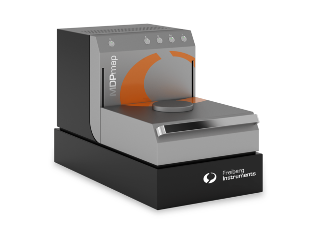
MDPmap

Skip breadcrumb navigation Breadcrumb Freiberg Instruments Products Microwave Detected Photoconductivity MDPmap MDPmap Precision Lifetime Charachterization with Exceptional Sensitivity Interested? Get in touch! Contact now Product Sheet Laser Selection Guide Skip menu Quick navigation Features Applications Specifications Technology Options Contact Advanced R&D – destruction free, flexible and fast Highly sensitive due to advanced microwave system Customized laser and optic integration for all your materials Simultaneous resistivity measurement and other options Materials The MDPmap features a versatile selection of advanced lasers, enabling comprehensive electrical characterization for nearly all types of semiconductors. Si SiC Ge GaAs Ga₂O₃ InP Diamond and more Features & Benefits 355–1550 nm Available wavelengths 10 ns Time resolution > 99 % repeatability Resistivity 0.3–5 Ohm cm Resistivity 0.3–5 Ohm cm Sensitivity: highest sensitivity for visualization of so far invisible defects and investigations of epitaxial layers Measurement speed: < 5 minutes for a 6 inch Si wafer, 1 mm resolution Range of lifetimes: 20 ns to several ms Contamination determination : metal (Fe) contaminations originated in crucibles and equipment Measurement capability: from as-cut wafers to fully processed samples Flexibility: fixed measurement head allows coupling of external lasers with trigger Reliability: modular and compact bench top instrument for higher reliability and uptime > 99% Repeatability: > 99% Resistivity: resistivity mapping without frequent calibration MDPmap - Mono-and Multi-crystalline wafer lifetime measurement device (µPCD/MDP(QSS)) Flexible mapping tool for R&D or production monitoring MDPmap is designed as a compact bench top contactless electrical characterization tool for offline production control or R&D, measuring parameters like carrier lifetime, photoconductivity, resistivity and defect information over a wide injection range in steady state or short pulse excitation (μ-PCD). Automated sample recognition and parameter setup allows an easy adaption to a big variety of different samples comprising epitaxial layers and wafers after various preparation stages ranging from as-grown wafers to up to 95% metallized ones. The major advantage of MDPmap is its high flexibility, which allows for instance the integration of up to four lasers either for injection level dependent lifetime measurements ranging from ultra low to high injection or extracting depth information by using different laser wavelengths. Bias light facility is included as well as options for μ-PCD or steady state injection conditions. A customer defined calculation with different maps is possible as well as an export of primary data for further evaluation. For standard metrology tasks a predefined standard enables routine measurements by only pushing one button. Lifetime map of passivated multicrystalline silicon Iron contamination map of multicrystalline silicon Bor oxygen map of mono silicon Trap density map of mono silicon Applications Photoconductivity measurements and trap analysis Equipped with a 355 nm laser (μ-PCD) or a 375 nm laser diode (MDP), the MDPmap as well as the MDpicts from Freiberg Instruments are suitable for photoconductivity measurements and trap analysis… Learn more Resistance measurements on wafers and bricks With MDPmap and MDPingot it is possible to measure the resistivity of wafers or bricks with a high accuracy and a resolution of 1 mm via eddy current measurements. The Eddy current sensor setup… Learn more Light Beam Induced Current (LBIC) The proceeding is based on the measurement of the local short circuit current Isc in the cell, which is produced through appropriate excitation. For the measurement the solar cell is contacted… Learn more Minority carrier Lifetime maps on 450 mm wafers Since several years, the microelectronic industry is planning to enlarge the wafer size from 300 mm (12 inch) to 450 mm (18 inch) diameter, in order to gain more yield. The technology for the… Learn more Iron concentration determination With the MDPingot and MDPmap series it is possible to measure the iron concentration in bricks and wafers fully automated and with a very high resolution. Lifetime measurements before and after… Learn more Minority carrier lifetime measurements on SiC In recent years the quality of SiC materials has improved profoundly and hence SiC is becoming more and more a competitor to Si for e.g. high-power devices. Since it is a wide-bandgap… Learn more Investigation of material quality of GaAs In contrast to other techniques MD-PICTS (microwave detected photo induced current transient spectroscopy) can detect signals even from thin surface regions (3 µm) of SI GaAs samples and is… Learn more Detection of CrB in silicon Lifetime measurements before and after chromium boron pair dissociation is a widely used method for chromium determination in silicon wafers. In boron doped silicon with a high doping… Learn more Detection of BO2 in silicon The boron-oxygen complexes can be activated by irradiating the sample with light and deactivated by heating the sample at 200 °C for several minutes. This can be used similar to the iron… Learn more Trap concentration determination With the MDPmap and MDPingot it is possible to measure the photoconductivity as well as the minority carrier lifetime with one measurement and fully automated in a wide injection range. A clever… Learn more Injection dependent measurements With MDPmap it is possible to measure not only injection dependent lifetime curves but also photoconductivity curves over a very wide range of injection. In the MDPmap and MDPingot up to 4… Learn more Highly spatial resolved inline metrology on Multicrystalline Silicon Non-destructive measurements of minority carrier lifetime are well established and widely used for process control and characterization of defects in crystalline silicon. With our tool MDPinline… Learn more Determination of passivation homogeneity and surface recombination vel The measured or effective lifetime consists of the bulk lifetime and the surface lifetime, via: \(\cfrac{1}{\tau_{eff}} = \cfrac{1}{\tau_{bulk}} + \cfrac{1}{\tau_{surface}}\) That‘s why the… Learn more Photoconductivity measurements of implanted samples In this case not the lifetime, but the photoconductivity or signal height is the most sensitive parameter for detecting inhomogeneity in implantations. It depends strongly on the resistivity and… Learn more Lifetime determination of epitaxial silicon thin-film layers With MDP it is possible to measure the lifetime of minority carriers and the photoconductivity in epitaxial layers as fast and exactly as possible with a high resolution. The measurement of… Learn more Interested? Our experts are happy to assist you. Get in touch! Contact us now! Technical specifications sample size up to 300 mm diameter (standard), up to 450 mm diameter (on request), down to 5 x 5 mm range of lifetimes 20 ns to several ms resistivity 0.2 - >10 3 Ohm cm, p/n material silicon wafer, epi layers, partially or fully processed wafers, compound semiconductors and beyond measureable properties lifetime - μ-PCD/MDP (QSS), photoconductivity excitation select up to four different wavelengths from 355 nm up to 1480 nm. 980 nm (default) dimensions 680 x 380 x 450 mm, weight: ca. 65 kg power 100 - 250V, 50/60 Hz, 5 A Technologies Minority carrier lifetime The measured effective lifetime is composed of the bulk lifetime and surface lifetime, which depends on the surface properties of a sample. Hence the surface has to be passivated, if you want… Learn more Photoconductivity When light of sufficient energy is absorbed by a semiconductor, the number of free electrons and holes changes and raises the electrical conductivity of the semiconductor. This increase is… Learn more Resistivity The electrical resistivity directly depends on the density of the semiconductor and is therefore a useful parameter to monitor doping profiles and homogeneity. The lifetime and diffusion length… Learn more Mobility The mobility is a quantity related to the drift velocity of electrons or holes in an applied electric field across a material. The mobility depends on different scattering processes that can… Learn more Diffusion length Learn more Defect properties The properties of a defect and its impact on the material quality can be described by three main parameters:defect concentration NT, capture cross sections for electrons and holes σn, σp,… Learn more Lifetime simulations From the simulated time dependent carrier concentrations the photoconductivity can be calculated using the mobility model of DORKEL and LETURCQ [2] . The minority carrier lifetime can be… Learn more Simulation of carrier profiles The measurement of thick samples as bricks leads to new questions and problems. One of these questions is how the carrier profiles that develops in a sample effect the lifetime measurements. To… Learn more Microwave detected photoconductivity (MDP) The novel method MDP is well suited for both, defect investigation by e.g. injection dependent minority carrier lifetime measurements, as well as mapping of wafers or even bricks for inline… Learn more Comparison to µ-PCD and QSSPC Besides MDP the two most important contact less lifetime measuring methods are QSSPC (quasi steady state photoconductivity) and µ-PCD (microwave detected photoconductive decay). Currently one… Learn more MD-PICTS MD-PICTS is a modification of MDP, where temperature dependent measurements of the defect part of the transient are accomplished. This allows for a spatially resolved defect characterization.… Learn more Penetration depth of different laser wavelength in silicon The microwave detected photoconductivity measures the photoconductivity after the irradiation of the sample with light. Usually the light should have an energy that is higher than the bandgap,… Learn more Materials Electrical properties and defects of a large variety of semiconductor materials, devices and dielectric materials can be investigated contact less and destruction with our advanced method MDP.… Learn more Accessories & Options Our devices offer versatile configuration options to meet specific requirements effectively. Each model can be customized to ensure maximum flexibility and efficiency. Contact for more information Spot size variation Resistivity measurement (wafers) Sheet resistance Background/Bias light Reflection measurement (MDP) LBIC for solar cells Reference wafer Internal/External iron mapping of Si Integrated heating stage Wide range of lasers Get in touch Do not hesitate to contact us – we are available to assist you with any inquiries or requests. Use our inquiry tool or reach out via email: sales @ freiberginstruments.com

Page

Automatic X-Y mapping stage

Skip breadcrumb navigation Breadcrumb Freiberg Instruments Products X-ray Diffraction Omega/Theta XRD Automatic X-Y mapping stage Automatic X-Y mapping stage for wafers and ingots Interested? Get in touch! Contact now The mapping stage allows to explore the whole sample surface using a controlled grid pattern. An Omega/Theta XRD can easily accommodate the additional xy-positioning stage on top of the turntable. The sample surface can be scanned according to a user-defined grid. The minimum grid spacing is about 1 mm, due to the size of the X-ray spot on the sample. The mapping stage can be combined with Omega Scan to get a crystal orientation mapping or with the rocking curve measurement to get a mapping of distortions on the surface. Software packages for display and analysis are available. YouTube Here you can find external content of the provider Google LLC. To be able to display these, we need your consent. privacy policy Show provider content Automatic X-Y mapping stage

Page

Omega/Theta - Rocking curve measurement

Skip breadcrumb navigation Breadcrumb Freiberg Instruments Products X-ray Diffraction Omega/Theta XRD Omega/Theta - Rocking curve measurement Omega/Theta - Rocking curve measurement Unique insights into lattice quality Interested? Get in touch! Contact now The Rocking Curve of a crystal reflection indicates the quality of the crystalline lattice. This can be down pointwise for fast checking or in combination with a mapping tool to receive a quality map. Measuring a Rocking Curve means measuring in Theta-scan mode, which requires a goniometer. A double crystal is brought into the primary beam path to decrease the spectral width and divergency. However, the side effect is a strongly reduced intensity. Therefore, the double crystal is mounted on a retractable holder to be able to switch it "on" or "off". Rocking curves of a 6H SiC crystal measured along a line on spots of 8 mm distance

Page

Omega/Theta - Customized sample holders

Skip breadcrumb navigation Breadcrumb Freiberg Instruments Products X-ray Diffraction Omega/Theta XRD Omega/Theta - Customized sample holders Customized sample holders Fixtures for tiny cylinders, large ingots or cubes for crystal orientation Interested? Get in touch! Contact now Sample stage for large samples for large samples up to 590 mm diameter max. sample mass = 30 kg additional fixtures for complex sample geometry on request Special holders for small samples fixing of small samples quick & easy sample placement simply exchangeable with other holder

Technology

Omega-scan

Omega-scan Ultra-Fast Orientation Measurement for Single Crystals Advantages of the Omega-Scan Method Stable and Simplified Setup The X-ray tube and detector remain fixed, requiring only a single measuring circle and no monochromator. Comprehensive Data Collection All necessary data for full orientation determination is captured in just one rotation. High Precision with Minimal Measurement Time The method delivers exceptional accuracy within a short measurement duration. These features make the Omega-Scan method particularly well-suited for routine measurements and industrial applications, where speed and reliability are essential. Understanding the Omega-Scan Method The Omega-Scan technique involves rotating the specimen 360° around a specific axis, such as the surface normal. The X-ray source and detector are positioned based on the crystal type to ensure an optimal number of reflections per turn. By analyzing the angular positions of these reflections, the crystal lattice orientation is determined in relation to the rotation axis. To precisely align the lattice orientation with the crystal surface, a laser beam checks the surface direction. Other relevant reference planes or directions can also be measured using optical tools. This technique enables accurate orientation measurement of single crystals in any configuration, achieving a reproducibility within a few arc seconds—often in just a few seconds of measurement. A specialized application of the Omega-Scan method is precision lattice-parameter determination , particularly for cubic crystals, providing highly accurate structural insights. Related Applications: Crystal Surface Orientation Mapping , 3D Mapping of Crystalline Turbine Blades , Quartz Bar Aligning , Automatic Wafer Sorting , Quartz Blank Sorting , Samples with a wide variety of geometry & size , Marking and measuring of in-plane directions , Crystal quality , NLO Materials: Crystal Quality & Optical Axis Orientation Matching Products XRD series Ingot XRD Enables existing equipment to reach high-end OD/Notch specs for 200 mm and 300 mm ingots Learn more XRD series Wafer XRD for fully automated sorting, sample crystalline orientation, sample dimension, optical notch/flat and edge profile determination and more Learn more XRD series Omega/Theta XRD for ultra-fast crystal orientation, crystal alignment in production, quality control, rocking curve measurements, material research and more Learn more XRD series DDCOM Ultra-fast, bottom surface measuring crystal orientation in a compact package Learn more XRD series SDCOM Ultra-fast, top surface measuring crystal orientation in a compact package Learn more XRD series XRD-OEM Fully automated in-line orientation and handling of ingots, boules, and pucks Learn more XRD series Ingot XRD SiC Enables existing equipment to reach high-end OD/Notch specs. Learn more XRD series Quartz Bar XRD Enable tight frequency specs in mass production Learn more XRD series Quartz Wafer XRD Enable tight frequency specs in mass production Learn more XRD series Quartz Blank XRD Enable tight frequency specs in mass production Learn more XRD series XRDmap Pro Inline wafer orientation mapping truly fab compliant Learn more XRD series Angle Sorter This product launching soon Learn more Get in touch Do not hesitate to contact us – we are available to assist you with any inquiries or requests. Use our inquiry tool or reach out via email: sales @ freiberginstruments.com

Technology

Theta-scan

Theta-scan Precision X-ray Method for Single Crystal Orientation Features of Theta-scan Pro allows to measure all crystalline materials, polytypes & orientations Contra at least 20 times slower than Omega-scan Advantages of this method are the relatively simple diffractometer alignment and its flexibility. The disadvantages are the rather long measurement time (some minutes) and the problem of finding enough reflections. Successful Theta Scans on at least two different lattice planes are needed to determine the complete crystal orientation. The reflections should be accessible to the diffractometer without moving the sample. Measurment procedure The angle between X-ray beam and detector is set to the reflection condition for a certain lattice plane that is given by the Bragg equation. To find the reflection, both X-ray and detector are moved coupled and simultaneously the sample is rotated. The direction of the lattice plane’s perpendicular is then calculated from the position of the reflection peak. There is no specific name for this method, thus we call it the "Theta-scan". Background: Bragg Equation The common XRD method for surface orientation determination is based on the Bragg equation: 2⋅ d ⋅sin(θ) = n ⋅λ which describes the relation between X-ray wavelength λ, lattice plane distance d , and the reflection glance angle θ. n indicates the diffraction order of the reflection. Related Applications: Crystal Surface Orientation Mapping , 3D Mapping of Crystalline Turbine Blades , Automatic Wafer Sorting Matching Products XRD series Wafer XRD for fully automated sorting, sample crystalline orientation, sample dimension, optical notch/flat and edge profile determination and more Learn more XRD series Omega/Theta XRD for ultra-fast crystal orientation, crystal alignment in production, quality control, rocking curve measurements, material research and more Learn more XRD series DDCOM Ultra-fast, bottom surface measuring crystal orientation in a compact package Learn more XRD series SDCOM Ultra-fast, top surface measuring crystal orientation in a compact package Learn more XRD series XRD-OEM Fully automated in-line orientation and handling of ingots, boules, and pucks Learn more XRD series Quartz Bar XRD Enable tight frequency specs in mass production Learn more XRD series Quartz Wafer XRD Enable tight frequency specs in mass production Learn more XRD series Quartz Blank XRD Enable tight frequency specs in mass production Learn more XRD series Angle Sorter This product launching soon Learn more Get in touch Do not hesitate to contact us – we are available to assist you with any inquiries or requests. Use our inquiry tool or reach out via email: sales @ freiberginstruments.com

Application

Marking and measuring of in-plane directions

Marking and measuring of in-plane directions with Omega-scan Efficient Crystal Orientation and In-Plane Direction Measurement with Omega Scan The Omega Scan provides a complete crystal orientation in a single measurement, allowing for the direct identification of in-plane directions. This feature is particularly useful for marking in-plane directions or verifying the orientation of flats and notches. During wafer implantation and photolithography, the flat or notch acts as an orientation marker. After processing, the wafer contains hundreds of chips that must be separated by cleaving. Correct alignment of these chips with a lattice plane is crucial for easy cleaving, making it necessary to check the position of the flat or notch. This requires precise measurement of in-plane components. Unlike the more complex or imprecise Theta Scan method, Omega Scan accurately measures the complete orientation in one go. The system also allows for easy adjustment of any in-plane direction to a specific position defined by the user, simplifying tasks such as flat orientation marking. For high-throughput applications, automated measurement solutions are available, ensuring maximum efficiency. Related Technologies: Omega-scan Matching Products XRD series DDCOM Ultra-fast, bottom surface measuring crystal orientation in a compact package Learn more XRD series SDCOM Ultra-fast, top surface measuring crystal orientation in a compact package Learn more XRD series Omega/Theta XRD for ultra-fast crystal orientation, crystal alignment in production, quality control, rocking curve measurements, material research and more Learn more Get in touch Do not hesitate to contact us – we are available to assist you with any inquiries or requests. Use our inquiry tool or reach out via email: sales @ freiberginstruments.com