Found 271 results in 1 milliseconds.

Application

Characterization of Ga2O3

Characterization of Ga2O3 Aim Ga 2 O 3 is an ultra-wide band gap semiconductor with a great application potential. The contactless characterization of defect related transitions with high sensitivity is still challenging. Solution Contactless surface photovoltage (SPV) spectroscopy in the dc (Kelvin probe, direct measurement of the contact potential difference, DCPD) and ac (modulated regime) modes provides information about transitions energies and direction of charge separation in a wide spectral range from near infrared (< 0.5 eV) up to the deep ultraviolet (> 6 eV) at high sensitivity. Furthermore, the same perforated electrode can be applied for measurements in dc and ac modes with a charge amplifier (figure 1). Application example Figure 2 shows an example for the measurement of a (negative) DCPD spectrum and the spectrum of the modulated SPV amplitude (in a logarithmic scale) on the same place of a b-Ga 2 O 3 crystal. Transitions at the band gap of b-Ga 2 O 3 at 4.8 eV and defect transitions at 1.6, 2.3, 3.2, 4.0, 4.4 and 4.6 eV are well distinguished whereas the sensitivities for measurements in the dc and ac modes can be rather different for different transitions. References [1] Th. Dittrich, S. Fengler, N. Nickel, “Surface photovoltage spectroscopy over wide time domains for semiconductors with ultrawide bandgap: example of gallium oxide”, Phys. Stat. Sol. A 11 (2021) 2100176. Fig. 1: Scheme for the measurement in dc and ac modes with the same electrode and a charge amplifier [1]. Fig. 2: Spectra of DCPD (blue) and spectrum of the modulated SPV amplitude (red) of a b-Ga2O3 crystal. Onsets at major defect transitions and at the band gap. Related Solutions and Industries: Epitaxial Layers & Thin Films Matching Products SPS/SPV series HR-SPSmap with fixed energy excitation sources High-Resolution and Sensitive Surface Photovoltage Measurement Solutions Learn more SPS/SPV series HR-SPSmap with variable energy excitation source with a variable energy excitation source Learn more Get in touch Do not hesitate to contact us – we are available to assist you with any inquiries or requests. Use our inquiry tool or reach out via email: sales @ freiberginstruments.com

Product

Comet2500

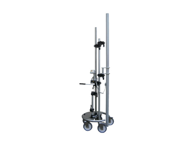
Skip breadcrumb navigation Breadcrumb Freiberg Instruments Products Radiation Monitoring Systems Comet2500 Comet 2500 Spatially resolved detector rod for shipping container measurement Interested? Get in touch! Contact now Skip menu Quick navigation Features Specifications Contact Features & Benefits Detector rod with gamma sensitive Geiger Müller tubes Local resolution through a serial line-up of 8 identical GM tubes Uniform sensitivity over the total length of the detector rod High gamma sensitivity for Co-60 with 18 cps per µSv/h Time saving and effective dose rate screening of transport containers Radioactivity check of floors and walls Track-down of “hot spots“ over a length of 2.5 m Technique 2 reliable Serial Micro Channels (each of variation SMC/QD) integrated in the detector rod Modular movable design with display and height adjustable detector rod High flexibility in its applications through vertical and horizontal positions of the detector rod Portable display und detector rod, simply with one hand (without tripod) 7“ color display with touch functions, resolution 800 x 480 pixels Distance measurement with laser meter mains or battery pack operation, accumulator charging at mains operation, energy management for battery pack control Get in touch Do not hesitate to contact us – we are available to assist you with any inquiries or requests. Use our inquiry tool or reach out via email: sales @ freiberginstruments.com

Page

Company

Company Innovation drives everything we do Driven by Innovation, Instruments Made to Measure We engineer and manufacture advanced measurement technologies and software solutions that redefine industry standards. Headquartered in Freiberg, Germany, we are a globally established leader with over 3,000 metrology systems worldwide. Our cutting-edge solutions serve dynamic industries like microelectronics, semiconductors, photovoltaics, chemicals, and medicine, delivering exceptional precision and unmatched efficiency. With ISO 9001:2015 certification, we prioritize quality and reliability at every step. We are Freiberg Instruments. We are driven by Innovation. Learn more about us Headquartered in Germany with more than 20 years of expertise +3,000 installations worldwide 20 years of expertise 11 sales offices worldwide +100 experts +100 experts We are Automation and Metrology Experts Our team of engineers, scientists, and professionals shares a relentless passion for excellence. Together, we have built a reputation for reliability, innovation, and exceptional customer service. We constantly redefines the limits of metrology. Meet the Team Career Opportunities Thesis and Internship Driving sustainability for a greener future Sustainability is at the core of Freiberg Instruments. We are committed to eco-friendly practices, targeted energy savings, and maintaining high occupational health and safety standards. Our roadmap aims for net-zero operations by 2030 and across the entire value chain by 2040. Together, we innovate responsibly for a greener, sustainable future. Read more Discover more Distributors & Partners Learn more Quality and Certification Learn more News Learn more Contact Learn more

Technology

Comparison between MPD and SPV techniques

Comparison between MPD and SPV techniques MDP (microwave detected photoconductivity): sensitive to moving photogenerated charge carriers (bulk property) SPV (surface photovoltage): sensitive to surface AND bulk properties with respect to ANY photogenerated charge carriers separated in space (moving or trapped) The MDP method does only apply to moderately doped semiconductors or close to perfect optical crystals The SPV method apply to any photoactive materials allowing for charge separation in space (semiconductors, multilayer and multijunction structures, molecular layers, powders) The MDP method can be modelled as a time dependent resistance measurement (DC), t MDP The SPV method can be modelled as a frequency and time dependent capacitance measurement (DC/modulation), t SPV For a non-ideal semiconductor (with defects), there can be a huge difference between the two methods, both methods provide complementary information about bulk and surface properties Matching Products SPS/SPV series HR-SPSmap with fixed energy excitation sources High-Resolution and Sensitive Surface Photovoltage Measurement Solutions Learn more SPS/SPV series HR-SPSmap with variable energy excitation source with a variable energy excitation source Learn more DPM series DPM100 Wide range double prism monochromator Learn more Get in touch Do not hesitate to contact us – we are available to assist you with any inquiries or requests. Use our inquiry tool or reach out via email: sales @ freiberginstruments.com

Technology

Comparison of PID Test Methods

Comparison of PID Test Methods A comparison with other widely used methods for PID testing demonstrates that the PIDcon has some unneglectable advantages The PIDcon test has the following advantages compared to other methods: Short duration (usually 4–8h) High variability: test of solar cell, mini-module, glass and EVA Good control of test especially in comparison to corona tests Very low costs per test PIDcon Vs. other test methods Matching Products PID series PIDcon bifacial Quality Control Solution for Bifacial PERC/PERC+, HIT, Topcon, c-Si Solar Cells, Mini Modules, and More Learn more Get in touch Do not hesitate to contact us – we are available to assist you with any inquiries or requests. Use our inquiry tool or reach out via email: sales @ freiberginstruments.com

Technology

Comparison to µ-PCD and QSSPC

Comparison to µ-PCD and QSSPC Among carrier lifetime experiments, it is still one of the biggest problems to understand widely contradicting results as obtained by different experimental methods. With our novel simulation tool it is possible to simulate steady state and non stead Besides MDP the two most important contact less lifetime measuring methods are QSSPC (quasi steady state photoconductivity) and µ-PCD (microwave detected photoconductive decay). Currently one of the biggest problems in the photovoltaic industry is to make the deviating lifetime measurement results of the different methods comparable. With our novel simulation tool it is possible to simulate steady state and non steady state measurements, so that a comparison is possible. µ-PCD The µ-PCD method typically operates at very high injections with a very short light pulse of only 200 ns. The minority carrier lifetime is determined via the photoconductive decay, similar to MDP. µ-PCD detects the photoconductivity by measuring the reflection of a microwave at the sample, which makes this method less sensitive than MDP. QSSPC QSSPC detects the changes in permeability of the sample and therefore the conductance via the coupling of the sample by a coil to a radio-frequency bridge. The exciting light is tuned down slowly, so that the sample is always in a quasi steady state. A further difference to MDP is the use of a flash-light with a hole light spectrum, in stead of monochrome laser light as the excitation source. Figure 1 displays the injection ranges in which the different lifetime measuring methods typically operate. It becomes clear that MDP surpasses the other methods, because it enables to measure over 7 decades of injection. If the measurement results of these different methods are compared, the injection, excitation wavelength, penetration depth of the microwave, the carrier profile and the different behaviour of traps, that depends on the duration of the light pulse, has to be taken into consideration. For more details read: [1] T. Hahn, Thesis, TU Bergakademie, 2009 Fig. 1: Comparison of MDP, µPCD and QSSPC with respect to their typical injection ranges Matching Products MDP series MDPmap Precision Lifetime Charachterization with Exceptional Sensitivity Learn more MDP series MDPspot Quick and Simple Lifetime Measurement Made Easy Learn more MDP series MDpicts pro High-Resolution, Temperature-Dependent Lifetime Measurement System for Precise Material Characterization Learn more MDP series MDPpro 850+ Advanced Solution for Quality Control of Monocrystalline Silicon Ingots, Bricks, and Wafers Learn more MDP series MDPlinescan Versatile OEM Unit for Lifetime Measurements on Silicon Samples, from Bricks to Processed Wafers Learn more MDP series MDpicts Temperature-Dependent Lifetime Measurement System for Advanced Material Analysis Learn more RES series RESmap High-Precision Resistivity Mapping System for Accurate Material Analysis Learn more Get in touch Do not hesitate to contact us – we are available to assist you with any inquiries or requests. Use our inquiry tool or reach out via email: sales @ freiberginstruments.com

Technology

Conductance Test and Power Loss

Conductance Test and Power Loss The conductance test and power loss are used to determine the pass/fail criteria for the PID test In order to establish an easy way to decide whether a solar cell or mini-module has a PID problem or not, even though the operator itself has not the physical background the power loss is determined and given as an output by the software PIDStudio. It shows the expected relative power loss of the degraded area of the cell under STC (1000 W/m 2 ) ∆P: Absolute power loss P 0 : Nominal power under standard test conditions (STC) = 1000 W/m 2 irradiance ∆P/P 0 : Relative power loss under STC conditions (approximate value, valid for power loss up to ~30%) V mpp : Voltage at maximum power (= 0.5 V for standard silicon solar cells) I mpp : Current at maximum power (= 8 A for standard silicon solar cells at STC) R p : Measured parallel resistance (= V/I as measured between front and back contact for the whole cell) A cell : Cell area (= 243 cm² for standard silicon solar cells) A pid : PID-tested area (= 100 cm² for standard PIDcon setup) Furthermore an easy pass or fail criterion after finishing the PID measurement is suggested. It is assumed that an efficiency loss of 3% at the end of the PID test lead to a fail of the solar cell (according to IEC-Standard). The measurement time therefore is 168 h at room temperature or 72 h at 85 °C (recipe “Long”). An efficiency loss of 3% is equal to an increase of the cell’s conductance of 150 mS for the tested area, meaning 1.5mS/cm 2 related to the 100 cm 2 electrode size. The formula for calculating the conductance is as follows: So it is the reciprocal of the parallel resistance related to the degraded area. If the PID diagram of a cell after 72 h shows a higher conductance increase as 1.5 mS/cm 2 , it fails the test and has a PID problem and should be sorted out, otherwise it will pass it. Please keep in mind that the test is not for absolute value of conductance, but only for increase of conductance (Conductance at the start point is unequal to zero). Please notice that the curves “Power loss” and “Conductance” look equal in the auto focus option, since the formulas are comparable. To save measurement time, the recommended measurement time is shortened to 4 hours. The fail criterion for that time span is 0.1 mS/cm 2 at 1000 V and 85 °C. Keep in mind that this criterion is only a hint for a PID problem, a conductance increase of 0.1 mS/cm 2 in 4 h will not lead to a measurable power loss. Therefore it is in the customer’s responsibility to check and use this fail criterion. Same applies for the recipe “Fast” with a fail criterion of 0.025 mS/cm 2 after 1 h. Nevertheless usage of higher measurement times (minimum 4 hours) is strongly recommended. Matching Products PID series PIDcon bifacial Quality Control Solution for Bifacial PERC/PERC+, HIT, Topcon, c-Si Solar Cells, Mini Modules, and More Learn more Get in touch Do not hesitate to contact us – we are available to assist you with any inquiries or requests. Use our inquiry tool or reach out via email: sales @ freiberginstruments.com

Page

Configuration options

Configuration options for lexsyg research Automatic detector changer The detector changer is fully automatic and software controlled. It can hold and change up to four different detectors like standard PMT, Red PMT, EMCCD, Spectrometry detection units, etc.… Learn more Irradiation sources Learn more Thermal stimulation Learn more Peltier cooling Low temperature conditions are used for radiation defect characterization. The system is capable of providing stable sample temperatures from -40 °C to -50 °C, while an automated change for high… Learn more Pulsed OSL (10 µs) Learn more Red stimulated quartz OSL Learn more Filter wheel Learn more PMT detection unit Learn more InfraRedPhotoLuminescence (IRPL) Compared to the standard IRSL the IRPL signal from K-feldspar is considered as probably being not, but certainly much less affected by fading (Prasad et. al. 2017). It also exhibits a larger dose… Learn more X-ray Fluorescence (XRF) This module allows an estimate of the mineral composition of feldspar samples. The relative proportion of K-/Na/-Ca-feldspar is estimated as well as the possible quartz contamination. The XRF… Learn more EMCCD UV to NIR (200 – 1050 nm) image detection for spatially resolved / single-grain measurement, operational at the TL/OSL or RF measurement position, 512 x 512 pixel back-thinned, UV-coated EMCCD… Learn more Sample camera The sample camera is designed to automatically record the appearance of the sample after luminescence measurements. For example:Visual inspection after luminescence data collection, Use of image… Learn more Spectrometry detection unit OE-CCD based high sensitivity spectrometry detection unit (Recommended for IR spectroscopy), fiber-coupled CCD based luminescence emission spectrometer, TE-cooled (min. -80 °C) CCD-detector 200… Learn more Bleaching/Solar simulation unit Features, power LED-array based light irradiator, fan-cooled, fully software controlled (power, irradiation time, mixing ratios - if applicable), within a measurement sequence the settings can be… Learn more Ultra-fast pulsing (< 10 ns) Module for fundamental studies on luminescence life-times and for separation of luminescence signals of different life-times by pulsed stimulation. Laser diode specifications:, Rise/fall time: <… Learn more

Page

Configuration options

Configuration options for lexsyg smart Irradiation sources The lexsyg TL/OSL reader can be equipped with up to 2 irradiation units. A sensor controlled mechanical shutter moved by air pressure provides repeatable, easy and safe functionality. Learn more Thermal stimulation (TL) Ceramic heating element allows highly reliable and more consistent measurements. The heating element is cooled by continuous flow of nitrogen or compressed air.Thermoluminescence (TL), preheat… Learn more Pulsed OSL (10 µs) All lexsyg smart and lexsygresearch TL/OSL readers can be equipped with an interchangeable OSL unit containing up to three stimulation wavelengths. These are provided by high power stimulation… Learn more Red stimulated quartz OSL Following Chruścińska et.al. (2018) and Palczewski & Chruścińska (2019) the stimulation of quartz at 620 nm allows a separation of the fast OSL component in thermally optically stimulated… Learn more Filter wheel Filter wheel including suitable filters, which are optimized for maximized luminescence light collection and maximum suppression of scattered light (OSL, PL) and thermal noise (TL), recommended… Learn more PMT detection unit Standard UV-VIS PMT unit (280 – 650 nm), standard detection unit for application in luminescence dating and dosimetry, bi-alkaline cathode PMT (HAMAMATSU H7360-02), sensitivity range: 300-650 nm,… Learn more Get in touch Do not hesitate to contact us – we are available to assist you with any inquiries or requests. Use our inquiry tool or reach out via email: sales @ freiberginstruments.com

Page

Contact

Contact Where innovation takes shape Freiberg Instruments is headquartered in Freiberg, in Silicon Saxony. Here, our experts in R&D, metrology, electronics, mechatronics, engineering, sales, and administration work hand in hand. We take pride in this close collaboration across disciplines and look forward to your visit! Find our global partners on the Distributors & Partners page. Get in touch Do not hesitate to contact us – we are available to assist you with any inquiries or requests. Use our inquiry tool or reach out via email: sales @ freiberginstruments.com Headquarters Freiberg Instruments GmbH Delfter Str. 6 09599 Freiberg Saxony, Germany Contact Mr. Ing. Thanga Kumar +49 3731 419 54 0 sales @ freiberginstruments.com View on Google Maps China Sales & Support Hub Freiberg Shanghai Instruments Co., Ltd. Room 602-2, Building 3, Lane 288, Qianfan Road 201600 Shanghai Songjiang District, China Contact Ms. Lu Yan +86-21-64200570 sales @ freiberginstruments.com.cn View on Google Maps Discover more Solutions Learn more Services Learn more Company Learn more