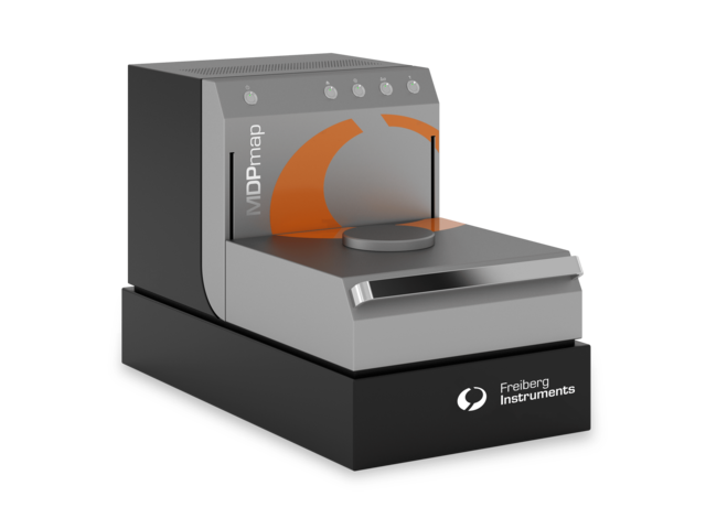
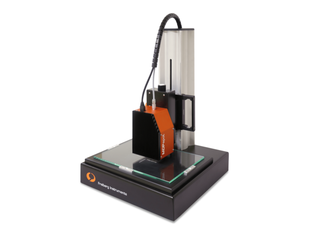
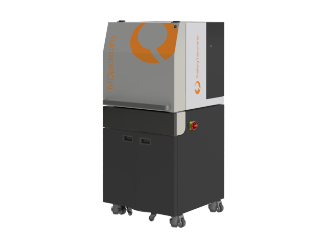
Skip breadcrumb navigation Breadcrumb Freiberg Instruments Products Microwave Detected Photoconductivity MDPmap MDPmap Precision Lifetime Charachterization with Exceptional Sensitivity Interested? Get in touch! Contact now Product Sheet Laser Selection Guide Skip menu Quick navigation Features Applications Specifications Technology Options Contact Advanced R&D – destruction free, flexible and fast Highly sensitive due to advanced microwave system Customized laser and optic integration for all your materials Simultaneous resistivity measurement and other options Materials The MDPmap features a versatile selection of advanced lasers, enabling comprehensive electrical characterization for nearly all types of semiconductors. Si SiC Ge GaAs Ga₂O₃ InP Diamond and more Features & Benefits 355–1550 nm Available wavelengths 10 ns Time resolution > 99 % repeatability Resistivity 0.3–5 Ohm cm Resistivity 0.3–5 Ohm cm Sensitivity: highest sensitivity for visualization of so far invisible defects and investigations of epitaxial layers Measurement speed: < 5 minutes for a 6 inch Si wafer, 1 mm resolution Range of lifetimes: 20 ns to several ms Contamination determination : metal (Fe) contaminations originated in crucibles and equipment Measurement capability: from as-cut wafers to fully processed samples Flexibility: fixed measurement head allows coupling of external lasers with trigger Reliability: modular and compact bench top instrument for higher reliability and uptime > 99% Repeatability: > 99% Resistivity: resistivity mapping without frequent calibration MDPmap - Mono-and Multi-crystalline wafer lifetime measurement device (µPCD/MDP(QSS)) Flexible mapping tool for R&D or production monitoring MDPmap is designed as a compact bench top contactless electrical characterization tool for offline production control or R&D, measuring parameters like carrier lifetime, photoconductivity, resistivity and defect information over a wide injection range in steady state or short pulse excitation (μ-PCD). Automated sample recognition and parameter setup allows an easy adaption to a big variety of different samples comprising epitaxial layers and wafers after various preparation stages ranging from as-grown wafers to up to 95% metallized ones. The major advantage of MDPmap is its high flexibility, which allows for instance the integration of up to four lasers either for injection level dependent lifetime measurements ranging from ultra low to high injection or extracting depth information by using different laser wavelengths. Bias light facility is included as well as options for μ-PCD or steady state injection conditions. A customer defined calculation with different maps is possible as well as an export of primary data for further evaluation. For standard metrology tasks a predefined standard enables routine measurements by only pushing one button. Lifetime map of passivated multicrystalline silicon Iron contamination map of multicrystalline silicon Bor oxygen map of mono silicon Trap density map of mono silicon Applications Photoconductivity measurements and trap analysis Equipped with a 355 nm laser (μ-PCD) or a 375 nm laser diode (MDP), the MDPmap as well as the MDpicts from Freiberg Instruments are suitable for photoconductivity measurements and trap analysis… Learn more Resistance measurements on wafers and bricks With MDPmap and MDPingot it is possible to measure the resistivity of wafers or bricks with a high accuracy and a resolution of 1 mm via eddy current measurements. The Eddy current sensor setup… Learn more Light Beam Induced Current (LBIC) The proceeding is based on the measurement of the local short circuit current Isc in the cell, which is produced through appropriate excitation. For the measurement the solar cell is contacted… Learn more Minority carrier Lifetime maps on 450 mm wafers Since several years, the microelectronic industry is planning to enlarge the wafer size from 300 mm (12 inch) to 450 mm (18 inch) diameter, in order to gain more yield. The technology for the… Learn more Iron concentration determination With the MDPingot and MDPmap series it is possible to measure the iron concentration in bricks and wafers fully automated and with a very high resolution. Lifetime measurements before and after… Learn more Minority carrier lifetime measurements on SiC In recent years the quality of SiC materials has improved profoundly and hence SiC is becoming more and more a competitor to Si for e.g. high-power devices. Since it is a wide-bandgap… Learn more Investigation of material quality of GaAs In contrast to other techniques MD-PICTS (microwave detected photo induced current transient spectroscopy) can detect signals even from thin surface regions (3 µm) of SI GaAs samples and is… Learn more Detection of CrB in silicon Lifetime measurements before and after chromium boron pair dissociation is a widely used method for chromium determination in silicon wafers. In boron doped silicon with a high doping… Learn more Detection of BO2 in silicon The boron-oxygen complexes can be activated by irradiating the sample with light and deactivated by heating the sample at 200 °C for several minutes. This can be used similar to the iron… Learn more Trap concentration determination With the MDPmap and MDPingot it is possible to measure the photoconductivity as well as the minority carrier lifetime with one measurement and fully automated in a wide injection range. A clever… Learn more Injection dependent measurements With MDPmap it is possible to measure not only injection dependent lifetime curves but also photoconductivity curves over a very wide range of injection. In the MDPmap and MDPingot up to 4… Learn more Highly spatial resolved inline metrology on Multicrystalline Silicon Non-destructive measurements of minority carrier lifetime are well established and widely used for process control and characterization of defects in crystalline silicon. With our tool MDPinline… Learn more Determination of passivation homogeneity and surface recombination vel The measured or effective lifetime consists of the bulk lifetime and the surface lifetime, via: \(\cfrac{1}{\tau_{eff}} = \cfrac{1}{\tau_{bulk}} + \cfrac{1}{\tau_{surface}}\) That‘s why the… Learn more Photoconductivity measurements of implanted samples In this case not the lifetime, but the photoconductivity or signal height is the most sensitive parameter for detecting inhomogeneity in implantations. It depends strongly on the resistivity and… Learn more Lifetime determination of epitaxial silicon thin-film layers With MDP it is possible to measure the lifetime of minority carriers and the photoconductivity in epitaxial layers as fast and exactly as possible with a high resolution. The measurement of… Learn more Interested? Our experts are happy to assist you. Get in touch! Contact us now! Technical specifications sample size up to 300 mm diameter (standard), up to 450 mm diameter (on request), down to 5 x 5 mm range of lifetimes 20 ns to several ms resistivity 0.2 - >10 3 Ohm cm, p/n material silicon wafer, epi layers, partially or fully processed wafers, compound semiconductors and beyond measureable properties lifetime - μ-PCD/MDP (QSS), photoconductivity excitation select up to four different wavelengths from 355 nm up to 1480 nm. 980 nm (default) dimensions 680 x 380 x 450 mm, weight: ca. 65 kg power 100 - 250V, 50/60 Hz, 5 A Technologies Minority carrier lifetime The measured effective lifetime is composed of the bulk lifetime and surface lifetime, which depends on the surface properties of a sample. Hence the surface has to be passivated, if you want… Learn more Photoconductivity When light of sufficient energy is absorbed by a semiconductor, the number of free electrons and holes changes and raises the electrical conductivity of the semiconductor. This increase is… Learn more Resistivity The electrical resistivity directly depends on the density of the semiconductor and is therefore a useful parameter to monitor doping profiles and homogeneity. The lifetime and diffusion length… Learn more Mobility The mobility is a quantity related to the drift velocity of electrons or holes in an applied electric field across a material. The mobility depends on different scattering processes that can… Learn more Diffusion length Learn more Defect properties The properties of a defect and its impact on the material quality can be described by three main parameters:defect concentration NT, capture cross sections for electrons and holes σn, σp,… Learn more Lifetime simulations From the simulated time dependent carrier concentrations the photoconductivity can be calculated using the mobility model of DORKEL and LETURCQ [2] . The minority carrier lifetime can be… Learn more Simulation of carrier profiles The measurement of thick samples as bricks leads to new questions and problems. One of these questions is how the carrier profiles that develops in a sample effect the lifetime measurements. To… Learn more Microwave detected photoconductivity (MDP) The novel method MDP is well suited for both, defect investigation by e.g. injection dependent minority carrier lifetime measurements, as well as mapping of wafers or even bricks for inline… Learn more Comparison to µ-PCD and QSSPC Besides MDP the two most important contact less lifetime measuring methods are QSSPC (quasi steady state photoconductivity) and µ-PCD (microwave detected photoconductive decay). Currently one… Learn more MD-PICTS MD-PICTS is a modification of MDP, where temperature dependent measurements of the defect part of the transient are accomplished. This allows for a spatially resolved defect characterization.… Learn more Penetration depth of different laser wavelength in silicon The microwave detected photoconductivity measures the photoconductivity after the irradiation of the sample with light. Usually the light should have an energy that is higher than the bandgap,… Learn more Materials Electrical properties and defects of a large variety of semiconductor materials, devices and dielectric materials can be investigated contact less and destruction with our advanced method MDP.… Learn more Accessories & Options Our devices offer versatile configuration options to meet specific requirements effectively. Each model can be customized to ensure maximum flexibility and efficiency. Contact for more information Spot size variation Resistivity measurement (wafers) Sheet resistance Background/Bias light Reflection measurement (MDP) LBIC for solar cells Reference wafer Internal/External iron mapping of Si Integrated heating stage Wide range of lasers Get in touch Do not hesitate to contact us – we are available to assist you with any inquiries or requests. Use our inquiry tool or reach out via email: sales @ freiberginstruments.com