Found 271 results in 2 milliseconds.

Application

Defects in 4H-SiC

Defects in 4H-SiC Investigated by surface photovoltage spectroscopy Defects in 4H-SiC investigated by surface photovoltage spectroscopy – power semiconductors Silicon carbide (SiC) high power, high voltage semiconductor devices lead the way not only for superfast chargers and on-board chargers for electrical vehicles (EV), but also power drive trains and power converters for traction applications such as light rails, trams and subways. Traction applications, as well as industrial motor drives, require power semiconductor switches with blocking voltages of 1200 V, 1700 V, 3300 V or even 4500 V (6500 V is still being explored). Reliability, lifetime and safety of the high power, high voltage semiconductor devices are the key parameters to control at the moment, where the commercially available 150 mm SiC wafers still suffer from some fundamental quality issues related to defects in bandgap of the SiC semiconductor. These issues will still remain on 200 mm SiC wafers, and it is therefore of extreme importance to be able to measure and report the state of the defects before, during and after device fabrication. The SPVcheck tool equipped with 3 UV light sources with centre wavelengths 355 nm, 365 nm and 450/660 nm is the ideal platform for epitaxial SiC wafer characterization, because it can be used to check the fundamental bandgap edge in a very elegant and fast way. The 450 nm or 660 nm wavelength is used as a baseline reference measurement, because the energy is too low to excite carriers in the SiC material. The 355 nm and 365 nm UV light sources are applied at the same time to the epitaxial SiC wafer, thereby creating a broad square like pulse covering energies in 3.25 to 3.55 eV in one shot. The transient SPV is measured in the time range from 10 ns and up to 10 ms. If the epitaxial layer on the SiC wafer has too many defects, the excitation of carriers will be weakened and the change in signal over time will be smaller. A perfect epitaxial layer, on the other hand, will have a higher output signal and, more importantly, sharp energy transition peaks in the ms range. An additional advantage of the square like energy pulse is the fact that the absorption coefficient of SiC is growing linearly with the square of the energy and is heavily temperature dependent. Therefore, by adding a temperature stage, the penetration depth of the UV light can be varied over a large range. Obviously the 355 nm and the 365 nm light sources does not need to switched on at the same time – they can be switched on and off in a modulated pattern with up to 1 kHz switching frequency or very long on and off cycles. Perfect 4H-SiC; Such a sharp transition will generate a large time-resolved signal change, probably around 10-100 µs 4H-SiC with defects; no sharp transitions will result in a small time-resolved signal change, probably < 1 µs Related Solutions and Industries: Epitaxial Layers & Thin Films Matching Products SPS/SPV series HR-SPSmap with fixed energy excitation sources High-Resolution and Sensitive Surface Photovoltage Measurement Solutions Learn more SPS/SPV series HR-SPSmap with variable energy excitation source with a variable energy excitation source Learn more Get in touch Do not hesitate to contact us – we are available to assist you with any inquiries or requests. Use our inquiry tool or reach out via email: sales @ freiberginstruments.com
Technology

Dependencies of PID Susceptibility

Dependencies of PID Susceptibility PID susceptibility is influenced by factors such as temperature, voltage, encapsulation materials, and the solar cell’s SiNx layer Temperature Higher heating plate temperatures lead to faster degradation of the solar cells. Unfortunately by using temperatures above 60 °C the EVA foil will irreparable damage the solar cell by conglutination. On the other hand simulates this lamination the situation of the module best. Voltage Usage of higher voltage is fastening the cell’s degradation. For fast degradation 1000 V are suggested, with 600 V differences between the cells are more finely graduated. It should be mentioned, that the voltage always is negative, so the PIDcon system is used for p-type cells. Humidity The influence of the humidity on the degradation result is insignificant, since the glass and EVA are press onto the solar cell and a full area contact is ensured. But if the cell is PID-resistant, small changes of humidity may result in small observable changes in the measured parallel resistance, since the contact resistance between the gold pins and the solar cell changes. Light Light has a huge impact on the PID measurement. It has to be ensured that the flap and the cover are closed during the measurement.Furthermore the positioning of strong light sources around the PIDcon device should be avoided. The diagram shows the influence on the resistance curve. For the first case the flap of the device was opened and closed, for the second one the cover was lifted to get a 5 mm gap to the ground plate and a strong illumination lamp was placed before the system and switched on and off. Glass and EVA From literature it is known that modules with quartz glas or alkali poor glas are not sensitive to PID-s. As shown in figure 1 also borat glas is well suited for modules which are stable against PID-s. Not necessary the Na concentration, but the resistivity of the glass from side to side is key for the PID susceptibility. Different encapsulation foils seem to be well suited for PID-s resistant modules(e.g. polyvinylbutyral (PVB), Thermoplastic silicon-elastomer (TPSE), Polyethylene (PE)). Similar to the glass a high resistivity of the polymer foil seems to lead to a PID resistant behavior. For more information please read: [1] V. Naumann, Ursachenanalyse und physikalische Modellbildung für potenzial-induzierte Degradation von Silizium-Solarzellen, Dissertation, Martin-Luther-Universität Halle-Wittenberg (2014) Matching Products PID series PIDcon bifacial Quality Control Solution for Bifacial PERC/PERC+, HIT, Topcon, c-Si Solar Cells, Mini Modules, and More Learn more Get in touch Do not hesitate to contact us – we are available to assist you with any inquiries or requests. Use our inquiry tool or reach out via email: sales @ freiberginstruments.com

Application

Detection of BO2 in silicon

Detection of BO2 in silicon Boron-oxygen complexes are one of the main reasons why solar cells degrade, when irradiated with sun light. Hence it is important to measure the boron-oxygen density in silicon fast, destruction free and with a high resolution. The boron-oxygen complexes can be activated by irradiating the sample with light and deactivated by heating the sample at 200 °C for several minutes. This can be used similar to the iron determination, to determine the relative boron-oxygen density by lifetime measurements before and after the activation and deactivation of the defect complex. The boron-oxygen density is determined via: \([BO_{2}] = C_{BO}(\Delta n) \cdot (\cfrac{1}{\tau_{BO}} - \cfrac{1}{\tau_{FeB}})\) For the boron-oxygen determination a calibration factor CBO is used, which depends on the injection and doping concentration. With the MDPmap and the heated sample stage a determination of the boron-oxygen concentration is possible for mc- and mono-Si with a high resolution. Related Solutions and Industries: Epitaxial Layers & Thin Films Matching Products MDP series MDPmap Precision Lifetime Charachterization with Exceptional Sensitivity Learn more MDP series MDPpro 850+ Advanced Solution for Quality Control of Monocrystalline Silicon Ingots, Bricks, and Wafers Learn more MDP series MDPpro Advanced Lifetime Measurement System for Quality Control and Material R&D on Semiconductors Learn more Get in touch Do not hesitate to contact us – we are available to assist you with any inquiries or requests. Use our inquiry tool or reach out via email: sales @ freiberginstruments.com

Application

Detection of CrB in silicon

Detection of CrB in silicon The determination of the chromium concentration is very important, since chromium is one of the most abundant and also most detrimental defects in silicon. (Alttext kürzen, da zu lang) Lifetime measurements before and after chromium boron pair dissociation is a widely used method for chromium determination in silicon wafers. In boron doped silicon with a high doping concentration, as it is used for PV applications nearly 100 % of the electrical active chromium is present as CrB pairs. With light of sufficient energy these pairs can be dissociated in Cri and B. This process is reversible and after some time all CrB pairs are associated again, which takes much longer as for FeB pairs. CrB and Cri have different recombination properties, so that the dissociation has an effect on the measured lifetime. With this effect the chromium concentration can be determined via: \([Cr] = C_{Cr}(\Delta n) \cdot (\cfrac{1}{\tau_{Cr}} - \cfrac{1}{\tau_{CrB}})\) For the chromium determination a calibration factor C is used, which depends on the injection and doping concentration. With the MDPmap and the heated sample stage a determination of the chromium concentration is possible for mc- and mono-Si with a high resolution. Related Solutions and Industries: Epitaxial Layers & Thin Films Matching Products MDP series MDPmap Precision Lifetime Charachterization with Exceptional Sensitivity Learn more MDP series MDPpro 850+ Advanced Solution for Quality Control of Monocrystalline Silicon Ingots, Bricks, and Wafers Learn more MDP series MDPpro Advanced Lifetime Measurement System for Quality Control and Material R&D on Semiconductors Learn more Get in touch Do not hesitate to contact us – we are available to assist you with any inquiries or requests. Use our inquiry tool or reach out via email: sales @ freiberginstruments.com

Application

Determination of passivation homogeneity and surface recombination vel

Determination of passivation homogeneity and surface recombination velocity For a lot of applications a well passivated surface is necessary e.g. in solar cells. With MDPmap and MDPingot it is possible to investigate the quality and homogeneity of the passivation with a high resolution. The measured or effective lifetime consists of the bulk lifetime and the surface lifetime, via: \(\cfrac{1}{\tau_{eff}} = \cfrac{1}{\tau_{bulk}} + \cfrac{1}{\tau_{surface}}\) That‘s why the surface properties, especially the surface recombination velocity S, has a huge influence on the measured lifetime. This can be used to investigate the surface properties of a sample. Thermal silicon oxide or SiN x are often used to passivate the surface of Cz- , Fz- or mc-Si, which means that the surface recombination velocity is minimized strongly. The homogeneity of this passivation layer can be investigated by lifetime measurements. The aim is to measure the homogeneity of a passivation layer with a high resolution. With MDPmap , MDPingot or MDPinline it is possible to investigate the homogeneity of a passivation layer with a very high resolution (only limited by the diffusion length of the carriers), which is exemplary shown in figure 1. Especially in high quality material with a high bulk lifetime the surface recombination is very dominant, so that every difference in a lifetime map has its origin in passivation inhomogeneity. By a measurement with different wavelength or different sample thickness even a good estimation of the surface recombination velocity can be made. If the sample quality is very high as in FZ-Si the surface recombination velocity can be determined from the measured lifetime by assuming that the bulk lifetime is only dependent on the Auger recombination. MDPmap , MDPingot or MDPinline enables to measure the homogeneity of a passivation layer with a very high resolution even inline. With this an optimization of the passivation process is possible. To approximate the bulk lifetime from the measured lifetime on unpassivated bricks, the following equation is used: \(\tau_{eff, \lambda} = \cfrac{\tau_{bulk}}{1-\alpha ^2L^2} \Biggl \lfloor 1-\alpha L\cfrac{\alpha L + \frac{SL}{D} coth \frac{\alpha d}{2}}{1 L + \frac{SL}{D} coth \frac{d}{2 L}} \Biggr]\) With d - sample thickness α - 1/penetration depth α = a/s (s – skin depth of the microwave; a – empiric factor, which was determined from comparison with passivated wafers from the same bricks) L – diffusion length D – diffusion coefficient S – surface recombination velocity for as cut surface (S = 2.0e+5) For further information please read: [1] J. Schmidt, Thesis, Universität Hannover, 1998 Fig. 1: Example of an oxide passivated Cz-Si wafer with a gradient in the oxide thickness Related Solutions and Industries: Epitaxial Layers & Thin Films , Photovoltaic , Research and Development Matching Products MDP series MDPlinescan Versatile OEM Unit for Lifetime Measurements on Silicon Samples, from Bricks to Processed Wafers Learn more MDP series MDPspot Quick and Simple Lifetime Measurement Made Easy Learn more MDP series MDPmap Precision Lifetime Charachterization with Exceptional Sensitivity Learn more MDP series MDPpro Advanced Lifetime Measurement System for Quality Control and Material R&D on Semiconductors Learn more Get in touch Do not hesitate to contact us – we are available to assist you with any inquiries or requests. Use our inquiry tool or reach out via email: sales @ freiberginstruments.com

Page

Diana Trinks

Diana Trinks Organizer, decision-maker and fire extinguisher Always striving forward, rethinking and developing something new from what we have learned. Diana Trinks Executive Assistant Diana has been an important pillar at Freiberg Instruments for over 13 years. As assistant to the management, she acts as a sparring partner and keeps the business running in the background with quick decisions. She previously worked in purchasing and warehousing. Diana, tell us about your first contact with FI. When I was looking for a new job, I spoke to my dancing girls from the carnival club. Mrs. Dornich, Kay's wife (founder and CEO), was one of them at the time. FI was looking for someone for the warehouse and purchasing - the challenge sounded exciting to me. I really enjoyed the trial working day. It was a new field for me, but it was exciting and a perfect interpersonal match. What do you associate with our guiding principle “Driven by Innovation”? Always striving forward, rethinking and developing new things from what we have learned. The guiding principle motivates us to keep inventing new, good and important things. What drives you? Whether it's visiting trade fairs, daily business or preparing evaluations - every day is different and presents new challenges. That's what motivates and drives me. What skills should a new colleague bring to your department? In a nutshell: A healthy dose of pragmatism is a great advantage. What are you particularly proud of? I didn't stop at my initial tasks. I have continued to develop and can therefore provide support in many areas wherever I am needed. How does FI support your professional development? I can concentrate on what I'm good at. I also receive various training courses that help me to become even better and sharpen my focus. What do you do to balance your job? I dance, enjoy spending time with my children and like to help out in my learned profession of gastronomy. Diana is Driven by Innovation Let's drive innovation together Current job openings Get to know the team Dr. Viktoriia Nikonova Productmanager Surface Photovoltage Spectroscopy Learn more Dr. Christian Hagendorf Projekt- & Key Account Manager XRD Series Learn more Martin Ferkinghoff Head of Service Learn more Marcus Richter Application & Service Engineer XRD Learn more Burkhard Winkler Senior Sales Engineer for semiconductors and automation Learn more Marcus Göhler Head of Electronics Development Learn more Thanga Kumar Global Sales Director Learn more Dr. Nadine Schüler Head of Research and Development Learn more

Technology

Diffusion length

Diffusion length Diffusion length The diffusion length is the average distance that the excess carriers can cover before they recombine. Diffusion length depends on the lifetime and mobility of the carriers. \(L = \sqrt{D\tau}\) Note: Diffusion factor (D) is not a constant, but depents on the carrier mobility. \(D = \mu \cfrac{kT}{e}\) For the resolution of every electrical measurement the diffusion length is the limitation. For a measurement of high quality silicon samples a maximal resolution of about 1 mm can be achieved. Matching Products MDP series MDPmap Precision Lifetime Charachterization with Exceptional Sensitivity Learn more MDP series MDPspot Quick and Simple Lifetime Measurement Made Easy Learn more MDP series MDpicts pro High-Resolution, Temperature-Dependent Lifetime Measurement System for Precise Material Characterization Learn more MDP series MDPpro 850+ Advanced Solution for Quality Control of Monocrystalline Silicon Ingots, Bricks, and Wafers Learn more MDP series MDPlinescan Versatile OEM Unit for Lifetime Measurements on Silicon Samples, from Bricks to Processed Wafers Learn more MDP series MDpicts Temperature-Dependent Lifetime Measurement System for Advanced Material Analysis Learn more RES series RESmap High-Precision Resistivity Mapping System for Accurate Material Analysis Learn more Get in touch Do not hesitate to contact us – we are available to assist you with any inquiries or requests. Use our inquiry tool or reach out via email: sales @ freiberginstruments.com

Page

Distributors & Partners

Distributors & Partners Trusted experts by your side – wherever you are We specialize in developing cutting-edge, customized technology. To ensure a seamless experience from first contact to purchase and beyond, we rely on a strong global network of experienced local partners. Our long-term distributors and partners share a close, trust-based relationship with us. They provide on-site support to help customers find and implement the perfect Freiberg Instruments solution and are always available for questions—wherever you need them. Headquarters Freiberg Instruments GmbH Delfter Str. 6 09599 Freiberg Saxony, Germany Contact Mr. Ing. Thanga Kumar +49 3731 419 54 0 sales @ freiberginstruments.com View on Google Maps Tech Sales & Semiconductor Metrology Consulting SemiSpin Snellius 1 6422RM Heerlen The Netherlands Contact Mr. Lars Grieger +49 1709454645 lars.grieger @ semispin.com View on Google Maps China Sales & Support Hub Freiberg Shanghai Instruments Co., Ltd. Room 602-2, Building 3, Lane 288, Qianfan Road 201600 Shanghai Songjiang District, China Contact Ms. Lu Yan +86-21-64200570 sales @ freiberginstruments.com.cn View on Google Maps Our Distributors in Asia India Ingeoserve Rajpur Road2nd Floor Shiva Palace Complex, 248001Dehradun India Contact Mr. Parmesh Sharma +91 9719001147 parmesh @ ingeoserve.com www.ingeoserve.com View on Google Maps Taiwan Challentech International Corporation No. 21, Taihe Rd 30267 Zhubei City Hsinchu County, Taiwan www.challentech.com.tw View on Google Maps Japan Correns Corporation 8-7, Roppongi 1-Chome2nd Dept. 3rd Business Div., Ark Yagi Hills Tokyo Minato-ku, Japan Contact Mr. Yuma Motohashi +81-3-5114-0778 y.motohashi @ correns.co.jp www.correns.co.jp View on Google Maps Singapore PL Nanotechnology PTE LTD 1 Raffles Place #44-02 One Raffles Place 048616Singapore Tower One, Singapore Contact Mr. Perry Lee +6593638706 info @ plnano.com www.PLNANO.com View on Google Maps South Korea ELIM GLOBALl Inc. #A1107, Bundang Suji U-Tower, 767 Sinsu-ro, Suji-gu 16827Gyeonggi-do South Korea Contact Mr. Han Eok Kim +82 31 7763 170 haneok.kim @ elim-global.com www.elim-global.com View on Google Maps Turkey SemiTech Semiconductor Technologies Konutkent Mah. 3035. Cd. Suit Tower A Blok No:89 06810Cankaya/Ankara Turkey Contact Mr. Mustafa Öztürk +90 312 999 6015 info @ semitech.com.tr www.semitech.com.tr View on Google Maps Turkey Merlab Laboratuvar Cihazlari San. Ve Tic. Limited Sti., 686 Sokak No. 72 Mustafa Kemal Mah. Buca-Izmir Turkey Contact Mr. Muhammet DEMIR +90-532-653-75-52 m.demir @ bentleymerkim.com.tr www.bentleymerkim.com.tr View on Google Maps Europe Germany RadPro International GmbH An der Hasenjagd 7 42897 Remscheid Contact Mr. Stefan Schischke +49 2191 6910415 s.schischke @ radproint.de www.radpro-int.com View on Google Maps North America United States Rotunda Scientific Technologies™ LLC 3732 Fishcreek Road Suite 913 44224 Stow Ohio, United States Contact Mr. Joe Rotunda +1 (330) 906-3403 joe @ rotundascitech.com www.RotundaSciTech.com View on Google Maps Our Partners Discover more About us Learn more Our people Learn more Quality and Certification Learn more News Learn more

Product

Dos'ASAP

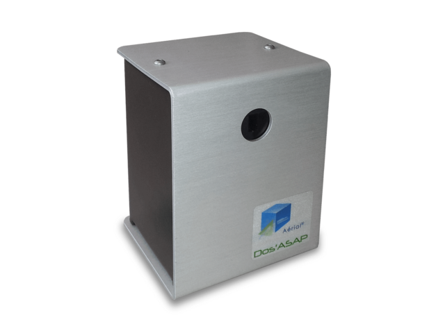
Skip breadcrumb navigation Breadcrumb Freiberg Instruments Products Luminescence Dating and Dosimetry Dos'ASAP Dos'ASAP PC-Controlled Dosimetry Device for CTA Readout, Compliant with ISO/ASTM Standards and FDA CFR 21 Part 11 Exclusively through Aerial CRT Contact for demo Skip menu Quick navigation Features Contact Highlights Photon and Electron Beam absorbed dose profile measurement (strip length from 5 cm to12 m) for dose uniformity estimation in user selected Region Of Interests (ROI) Electron Beam energy determination with wedge technique according to ISO/ASTM 51649 Electron Beam scan width, scan length and scanning uniformity assessment and many more Features & Benefits Dos’ASAP is a PC controlled dosimetry device for CTA dosimeter readout. Its control software is data base driven and compliant with relevant standards (ISO/ASTM 51649, 51650, 51261, ISO 11137-3,...) and FDA CFR 21 part 11. Dos'ASAP – Exclusively through Aerial CRT, France Contact Mr. Florent Kuntz Contact now Dos'ASAP – Exclusively through Aerial CRT, France Contact Mr. Florent Kuntz Contact now

Page

Double Prism Monochromator

Double Prism Monochromator Unlock the Future of Spectral Analysis: The DPM series Experience unparalleled optical performance with our state-of-the-art Wide-Range Double Prism Monochromator — engineered to deliver exceptional spectral precision, broad wavelength coverage, and ultra-low stray light levels. Designed for demanding applications in photonics, analytical chemistry, and materials science, this advanced system features dual-prism technology that ensures seamless tunability and high throughput across an extended spectral range. Whether you're an experienced researcher or just beginning your scientific journey, the monochromator’s user-friendly interface and robust design make it easy to integrate into any workflow — boosting productivity and accelerating innovation. DPM series DPM100 Learn more With its double prism design, the DPM100 outperforms standard grating monochromators by offering a broader spectral range from UV to NIR – ideal for high-precision and flexible spectroscopy. Ing. Thanga Kumar Sales Director Discover more of the DPM series Publications Learn more Get in touch Do not hesitate to contact us – we are available to assist you with any inquiries or requests. Use our inquiry tool or reach out via email: sales @ freiberginstruments.com