Found 271 results in 2 milliseconds.

Application

Advanced identification of polymers and semiconductors

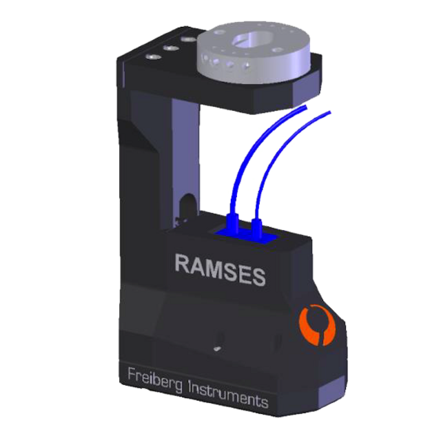
Advanced identification of polymers and semiconductors Aim Polymers and semiconductors are highly functional materials, and major components of electronic and electrical products. Their detailed characteristics are key to validate functionality and ensure adequate treatments both in manufacturing and post-consumer management stages of their life cycle. An automated, contact-free and non-destructive sensing solution can provide the framework for real-time industrial operations, as needed in various applications in the fields of production and waste management (i.e. recycling). Solution Raman spectroscopy measurements provide a powerful solution for detecting the detailed composition of both polymers and semiconductor materials. For polymers, Raman spectra contain the information needed to identify not only key polymer types (e.g. PE, PP, ABS, PS, PC, PET, PVC, PMMA), but to also overcome the challenging identification of black polymers, additives and polymer blends relevant for high quality sorting, recycling and quality control. For semiconductors, information from Raman measurements can detect the type of semiconductor (e.g. Si, Si-C, Sapphire), including the presence and type of dopants. Short integration times, combined with the possibility of robotic integration, allow for agile sensing solutions in dynamic settings such as on top of conveyor belts. The main advantages of our Raman measurement head are: Selection of different laser powers + integration times allow for Identification of several material streams which are unresolved by current solutions (challenging complex polymers, Identification of semiconductor type and presence/type of dopants). Possibility of sensor integration to robotic arms with automatic shutter and interlock signal for security Possibility of robot-based operation in a sensor network for high-throughput advanced classification of complex materials (linked to invention disclosure and patent application). software interface for selecting ‘recipes’ of different laser power/integration times according to each stream Application example Raman measurements have been conducted in the dynamic setting of conveyor belt-based material stream characterization. Under ambient light conditions, the diagnostic fingerprints of major polymer types could be recorded down to 0,5 s integration time with an adequate signal to noise ratio which allows for their identification (see Fig. …). Laser power can be tuned according to the needs of selected material types, ensuring optimal signal acquisition for multiple material streams. For more comprehensive material stream characterization, it is possible to integrate the robot-compatible Raman sensor with further imaging sensors (e.g. RGB and reflectance-based hyperspectral cameras). In such a complex, integrated system, a robot-mounted Raman solution provides a myriad of tailor-based options for boosting the accuracy of results and widens the range of detectable materials. Fig 1. Raman spectra collected from ABS-white (top) and ABS-black (bottom) plastic standards. Acquisition times from 250–500 ms. Identification of ABS is key in electronic waste recycling, as the material shares spectral features with other styrenic polymers in VNIR-SWIR (sensor most commonly used in the plastic recycling industry). Particularly, allows for the differentiation between ABS and PS polymers. Identification of polymer fingerprints from signals acquired at fast acquisition times (maximum: 500 ms). Successful use of recipes for signal acquisition of samples of the same plastic type, but with different colours (white-ABS vs black-ABS). Acquisition of polymer-specific features in samples with white pigments and broad fluorescence bands (from 1600–2000 cm-1) -> ABS white Acquisition of polymer-specific features in samples with black pigments and high absorption of excitation light, without damaging the material -> ABS black (500 ms acquisition time). Highlight: measurement conditions suitable for real-time and dynamic settings short integration time and tunable laser power Fig. 2. Raman spectra collected from HDPE-transparent (top) and HDPE-black (bottom) plastic standards. Acquisition time: 500 ms. Identification of diagnostic HDPE-diagnostic features in both transparent and black standards. HPDE transparent: no influence from the background materials are observed in the final spectra (this means that the presence of a conveyor belt or another dark-colour background doesn’t impact the signal collection. HDPE black: depending on the amount of dark pigments and other absorbers, signal acquisition may be impacted (see low SNR for PE-2 feature). Still, the other PE-related fingerprints exhibited good SNR, which allow for identification of the polymer type even under limiting conditions. Example for identification of semiconductor type (Si and 4H-SiC) using the RAMSES measurement head. Matching Products RAMSES RAMSES-4-CE Fully automated, high sensitive Raman Sensor for polymer and semiconductor sorting Learn more Get in touch Do not hesitate to contact us – we are available to assist you with any inquiries or requests. Use our inquiry tool or reach out via email: sales @ freiberginstruments.com
Product

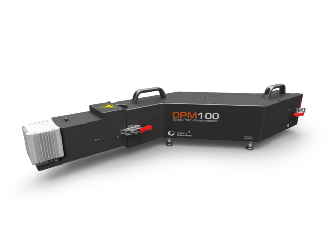
DPM100

Skip breadcrumb navigation Breadcrumb Freiberg Instruments Products Double Prism Monochromator DPM100 DPM100 Wide range double prism monochromator Interested? Get in touch! Contact now Product Sheet Skip menu Quick navigation Features Technology Contact Enables the adjustment of the wavelength over a wide spectral range without any discontinuities Extremely wide spectral range (0.4–7.3 eV/ 170 - 3100 nm) Spectral resolution: 2 meV – 100 meV (depending on wavelength and slit width) Excellent stray light suppression Materials The DPM100 can be used for all kinds of materials Si SiC Ge GaAs Ga₂O₃ InP Diamond and more Features & Benefits 0.4–7.3 eV Spectral range >10⁸ Stray light suppression 3 mm Spot diameter 2–100 meV Spectral resolution 2–100 meV Spectral resolution Interested? Our experts are happy to assist you. Get in touch! Contact us now! Technologies Electrical and optical characterization using surface photovoltage spe Photocarrier generation and separation mechanisms, Minority carrier lifetime measurement/Diffusion length calculations, Trapped carrier dynamics, time resolved, Surface Photovoltage… Learn more SPV signal analysis: fits and simulations We are currently developing simulation tools to enable first principle calculations of the electronic structure in a given photoactive material or material combination, based on solid-state… Learn more Comparison between MPD and SPV techniques MDP (microwave detected photoconductivity): sensitive to moving photogenerated charge carriers (bulk property), SPV (surface photovoltage): sensitive to surface AND bulk properties with respect… Learn more Static, transient or modulated light excitation pro and con The time-resolved or frequency-modulated, surface photovoltage spectroscopy (SPS) is based on a time-resolved/frequency modulated measurement of the spectral dependence of the surface… Learn more SPV-Picts SPV temperature dependence measurements Use this option to make SPV measurements at different temperatures between room temperature and 200°C. Temperature-dependent SPV measurements can be applied to measure activation energies or to… Learn more Materials Any photoactive material from raw material to finished device:From powder-based samples over wafers to boules or ingots. From 10 x 10 mm2 and up to 300 mm diameter, From titanium dioxide over… Learn more Get in touch Do not hesitate to contact us – we are available to assist you with any inquiries or requests. Use our inquiry tool or reach out via email: sales @ freiberginstruments.com
Application

High precision Resistivity Measurement

High precision Resistivity Measurement on highly doped semiconductors Aim Measuring resistivity in highly doped semiconductors is crucial for several reasons: Quality control and Doping density verification Device performance prediction Extraction of material parameters as mobility and carrier concentration Process development (e.g. ion implantation) and simulation of doping models Detection of contaminations, process drift and inhomogeneities and defects as the growth facet in SiC for the Laser splitting process of SiC Hence precision and reproducibility are critical for advanced semiconductor applications. Solution The RESmap from Freiberg Instruments enables high-precision mapping of all kinds of highly doped materials (Si, SiC and more) in a range of 1 to 100 mΩcm with an unsurpassed repro-ducibility (σ < 0.15 %) due to the integrated distance and temperature sensors and the sensitive measurement head. This compact measurement head can also be used as a hand-held tool, it is available in a fully automated version with robot handling or can be integrated into the production line. Application example Figure 1 shows an exemplary mapping of the resistivity of a SiC raw wafer. The edge exclusion is appr. 5 mm. It is well known that the measured resistivity depends on the sample temperature, but also on the ambient temperature. Hence two T sensors are integrated in the measurement head. Figure 2 shows 1000 repeats of a resistivity measurement at a thick SiC boule (> 1 mm). The measurement head was driving in the home position after every measurement and the complete procedure took around 6 hours. In this time the ambient temperature changed and this test shows nicely how well the T com-pensation algorithm works. A reproducibility with s < 0.15 % is achieved with this T compensation algorithm. Figure 1: Example of a resistivity map of a SiC wafer For the cold laser splitting process for SiC also the crystal orientation is extremely important. Freiberg Instruments offers a lot of solutions for a fast and precise measurement of the crystal orientation, which can be tailored to your individual process line. Please check out our XRD solutions. Figure 2: 1000 repeats with movement to home position; with (σ < 0.15 %) and without temper-ature compensation (σ < 0.21 %) Figure 3: average of a 5 mm map of a 6’’ boule, measured 18 times on different days and differ-ent times, σ = 0.15 % Figure 4: dynamic temperature drift: sample was placed at a cold spot and measured during the warm up, the experiment took about 10 mins Matching Products RES series RESmap High-Precision Resistivity Mapping System for Accurate Material Analysis Learn more Get in touch Do not hesitate to contact us – we are available to assist you with any inquiries or requests. Use our inquiry tool or reach out via email: sales @ freiberginstruments.com

Page

Resistivity Mapping

Resistivity Mapping Accurate Material Analysis for Semiconductor Quality Control: The RES series Advanced resistivity mapping is essential for semiconductor quality control across materials like SiC, GaN, InP, and more. Using eddy-current sensing, it enables non-contact, high-precision measurements with excellent repeatability (σ < 0.15%), even on complex shapes such as wafers, boules, and ingots. Integrated distance and temperature sensors ensure stable, accurate results by compensating for external and material-related variations. Automation in resistivity mapping has significantly increased throughput and reduced manual intervention. With X-Y mapping capabilities and multi-point measurement resolution as fine as ±0.1 mm, these systems are optimized for both research labs and high-volume manufacturing. Easy calibrating routines and compatibility with industry standards like SEMI MF 673 help streamline setup and maintain long-term system performance. Combining high sensitivity, automation, and broad material compatibility, this technology supports a wide range of semiconductor applications—helping manufacturers improve yield, accelerate development, and scale with confidence. RES series RESmap Learn more The market launch of RESmap was a special milestone – a game changer for the semiconductor industry. Dr. Christian Hagendorf Key Account Manager Get in touch Do not hesitate to contact us – we are available to assist you with any inquiries or requests. Use our inquiry tool or reach out via email: sales @ freiberginstruments.com

Page

Double Prism Monochromator

Double Prism Monochromator Unlock the Future of Spectral Analysis: The DPM series Experience unparalleled optical performance with our state-of-the-art Wide-Range Double Prism Monochromator — engineered to deliver exceptional spectral precision, broad wavelength coverage, and ultra-low stray light levels. Designed for demanding applications in photonics, analytical chemistry, and materials science, this advanced system features dual-prism technology that ensures seamless tunability and high throughput across an extended spectral range. Whether you're an experienced researcher or just beginning your scientific journey, the monochromator’s user-friendly interface and robust design make it easy to integrate into any workflow — boosting productivity and accelerating innovation. DPM series DPM100 Learn more With its double prism design, the DPM100 outperforms standard grating monochromators by offering a broader spectral range from UV to NIR – ideal for high-precision and flexible spectroscopy. Ing. Thanga Kumar Sales Director Discover more of the DPM series Publications Learn more Get in touch Do not hesitate to contact us – we are available to assist you with any inquiries or requests. Use our inquiry tool or reach out via email: sales @ freiberginstruments.com

Product

RAMSES-4-CE

Skip breadcrumb navigation Breadcrumb Freiberg Instruments Products Raman Sensor RAMSES-4-CE RAMSES-4-CE (Raman Sensor) Fully automated, high sensitive Raman Sensor for polymer and semiconductor sorting Interested? Get in touch! Contact now Skip menu Quick navigation Features Applications Contact A powerful solution for detecting the detailed composition of both polymers and semiconductor materials Selection of different laser powers + integration times allow for Identification of several material streams Possibility of sensor integration to robotic arms with automatic shutter and interlock signal for security Software interface for selecting ‘recipes’ of different laser power/integration times according to each stream Materials Polymers esp. black plastics and semiconductors Features & Benefits Identification of black plastics Acquisition times of maximum 500 ms Recipe based for different material streams Suitable for real time sorting Applications Advanced identification of polymers and semiconductors Polymers and semiconductors are highly functional materials, and major components of electronic and electrical products. Their detailed characteristics are key to validate functionality and… Learn more Get in touch Do not hesitate to contact us – we are available to assist you with any inquiries or requests. Use our inquiry tool or reach out via email: sales @ freiberginstruments.com

Product

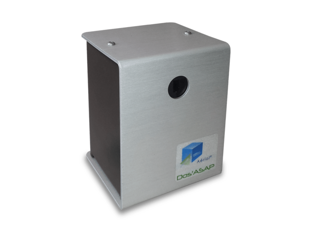
Dos'ASAP

Skip breadcrumb navigation Breadcrumb Freiberg Instruments Products Luminescence Dating and Dosimetry Dos'ASAP Dos'ASAP PC-Controlled Dosimetry Device for CTA Readout, Compliant with ISO/ASTM Standards and FDA CFR 21 Part 11 Exclusively through Aerial CRT Contact for demo Skip menu Quick navigation Features Contact Highlights Photon and Electron Beam absorbed dose profile measurement (strip length from 5 cm to12 m) for dose uniformity estimation in user selected Region Of Interests (ROI) Electron Beam energy determination with wedge technique according to ISO/ASTM 51649 Electron Beam scan width, scan length and scanning uniformity assessment and many more Features & Benefits Dos’ASAP is a PC controlled dosimetry device for CTA dosimeter readout. Its control software is data base driven and compliant with relevant standards (ISO/ASTM 51649, 51650, 51261, ISO 11137-3,...) and FDA CFR 21 part 11. Dos'ASAP – Exclusively through Aerial CRT, France Contact Mr. Florent Kuntz Contact now Dos'ASAP – Exclusively through Aerial CRT, France Contact Mr. Florent Kuntz Contact now

Page

Raman Sensor

Raman Sensor RAMSES RAMSES-4-CE Learn more Discover more of the RAMSES series Applications Learn more Get in touch Do not hesitate to contact us – we are available to assist you with any inquiries or requests. Use our inquiry tool or reach out via email: sales @ freiberginstruments.com

Page

Applications

RAMSES Aplications Advanced identification of polymers and semiconductors Learn more

Page

Applications

RESmap Applications High precision Resistivity Measurement Learn more