Found 271 results in 1 milliseconds.

Product

Ingot XRD SiC

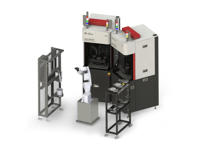
Skip breadcrumb navigation Breadcrumb Freiberg Instruments Products X-ray Diffraction Ingot XRD SiC Ingot XRD SiC Enables existing equipment to reach high-end OD/Notch specs. Interested? Get in touch! Contact now Skip menu Quick navigation Features Technology Software Contact Revolutionize your ingot post glueing preparation: Automated, precise and modular Ultra-fast hybrid X-ray optical metrology with proprietary algorithm Robot driven operations with modular metrology and tooling Advanced factory connectivity and service provisions Materials The Ingot XRD SiC delivers high-throughput and precision for the efficient production of advanced SiC wafers. SiC GaN AIN and more Features & Benefits Unmatched Quality with hybrid metrology 0.005˚ On-axis precision Flexible Loading and communication options Diameter 100–300 mm Diameter 100–300 mm Interested? Our experts are happy to assist you. Get in touch! Contact us now! Technologies Omega-scan Ultra-Fast Orientation Measurement for Single Crystals Learn more Software XRDStudio Multiple Operating ModesOperator Mode: Designed for fixed measurement parameters, ensuring a safe and streamlined workflow. Administrator Mode: Allows for the creation and modification of… Learn more Get in touch Do not hesitate to contact us – we are available to assist you with any inquiries or requests. Use our inquiry tool or reach out via email: sales @ freiberginstruments.com

Application

Injection dependent measurements

Injection dependent measurements The minority carrier lifetime is strongly dependent on the injection (excess carrier concentration). From the shape and height of the lifetime curve information about the dominant recombination center as well as trapping center can be deduced. With MDPmap it is possible to measure not only injection dependent lifetime curves but also photoconductivity curves over a very wide range of injection. In the MDPmap and MDPingot up to 4 different lasers can be integrated and hence it is possible to measure not only injection dependent lifetime curves but also photoconductivity curves over a very wide range of injection. Figure 1 displays a comparison of the typical injection range of different known lifetime measuring methods. Because of its extraordinary sensitivity the MDPmap and MDPingot are able to measure over seven decades of injection. Due to bias light and reflection measurements a very good accuracy could be improved profoundly. With MDPmap the whole important injection range can be covered with just one method as demonstrated in figure 2 for 2 different spots on a SiNx passivated mc-Si wafer. Until now it was necessary to use several different methods, which often cannot be compared to each other. With MDP an easy excess to the important injection dependent lifetime curves is possible. For further information please read: [1] S. Rein, Lifetime Spectroscopy - A Method of Defect Characterization in Silicon for Photovoltaic Applications , Vol. 85 (Springer, Berlin Heidelberg, 2005) Bulklifetime versus injection for a varying symmetry factor and energy level Fig. 1: Comparison of typical injection ranges of different measuring methods Fig. 2: injection dependent lifetime measurements on 2 different spots on a SiNx passivated mc-Si wafer Related Solutions and Industries: Epitaxial Layers & Thin Films Matching Products MDP series MDPmap Precision Lifetime Charachterization with Exceptional Sensitivity Learn more MDP series MDPspot Quick and Simple Lifetime Measurement Made Easy Learn more MDP series MDPpro 850+ Advanced Solution for Quality Control of Monocrystalline Silicon Ingots, Bricks, and Wafers Learn more MDP series MDPpro Advanced Lifetime Measurement System for Quality Control and Material R&D on Semiconductors Learn more Get in touch Do not hesitate to contact us – we are available to assist you with any inquiries or requests. Use our inquiry tool or reach out via email: sales @ freiberginstruments.com

Application

Inline metrology of mc-Si bricks

Inline metrology of mc-Si bricks Lifetime measurements are already widely used for material quality control especially in the photovoltaic industry. Taking it one step further, (Alttext zu lang) With the MDPinline ingot it is possible to measure all 4 sides of a brick in under 1 min per side with 1 mm resolution. At the same time a spatial resolved measurement of conduction type changes as well as resistivity linescans are measured. Customer defined brick cut criteria by lifetime, resistivity or conduction type change can be transmitted to the fab database, which allows a fully automated material monitoring for next generation photovoltaic fabs. Furthermore the iron density can be measured on one side of the brick, which takes about 2.5 min. Related Solutions and Industries: Epitaxial Layers & Thin Films Matching Products MDP series MDPpro 850+ Advanced Solution for Quality Control of Monocrystalline Silicon Ingots, Bricks, and Wafers Learn more MDP series MDPpro Advanced Lifetime Measurement System for Quality Control and Material R&D on Semiconductors Learn more Get in touch Do not hesitate to contact us – we are available to assist you with any inquiries or requests. Use our inquiry tool or reach out via email: sales @ freiberginstruments.com

Application

Investigation of defect levels in InP

Investigation of defect levels in InP InP is applied in high frequency technique, for lasers, communication technique and production of integrated circuits. Hence also for this material methods for defect investigation and quality control are needed. MD-PICTS is a well suited method for the investigation of defect levels in InP. For example investigations on indium phosphide shows that the defect content changes during annealing processes, which may also have an impact on the distribution of electric properties. Whereas the defect content of as-grown samples depends on their position in the crystal, an equivalent set of defect levels is prominent in wafer-annealed samples. Figure 1 shows a comparison of Fe-doped SI-InP samples from different crystal positions. They differ in their characteristic defect levels. The observed peaks in FE-doped InP provided the first proof of iron acting as a recombination center in InP. Fig.1: Comparison of MD-PICTS spectra of as-grown Fe doped SI-InP samples from different crystal positions and thus different FE concentrations. The samples differ in their characteristic defect levels Related Solutions and Industries: Epitaxial Layers & Thin Films Matching Products MDP series HTpicts Advanced High-Temperature Lifetime Measurement System for In-Depth Material Analysis Learn more MDP series MDpicts pro High-Resolution, Temperature-Dependent Lifetime Measurement System for Precise Material Characterization Learn more MDP series MDpicts Temperature-Dependent Lifetime Measurement System for Advanced Material Analysis Learn more Get in touch Do not hesitate to contact us – we are available to assist you with any inquiries or requests. Use our inquiry tool or reach out via email: sales @ freiberginstruments.com

Application

Investigation of material quality of GaAs

Investigation of material quality of GaAs Besides silicon GaAs is one of the most important materials in modern technology and therefore a method to investigate the material quality is needed. (Alttext kürzen, da zu lang) In contrast to other techniques MD-PICTS (microwave detected photo induced current transient spectroscopy) can detect signals even from thin surface regions (3 µm) of SI GaAs samples and is therefore able to analyze e.g. influence of surface treatments. Figure 1 shows the defect peak of the well-known EL2 defect in samples with different acceptor concentrations. Fig. 1: Detection of the EL2 defect in SI GaAs samples with different acceptor concentrations by MD-PICTS, peak height and sign correlate to the acceptor concentration Related Solutions and Industries: Epitaxial Layers & Thin Films Matching Products MDP series MDPmap Precision Lifetime Charachterization with Exceptional Sensitivity Learn more MDP series MDPspot Quick and Simple Lifetime Measurement Made Easy Learn more MDP series MDpicts Temperature-Dependent Lifetime Measurement System for Advanced Material Analysis Learn more Get in touch Do not hesitate to contact us – we are available to assist you with any inquiries or requests. Use our inquiry tool or reach out via email: sales @ freiberginstruments.com

Application

Investigation of photocatalytic materials (BiVO4)

Investigation of photocatalytic materials (BiVO4) Aim Photocatalytic materials such as BiVO 4 are of great interest, for example, for water splitting. Electronic defect states and surface passivation are important limiting factors. Photocatalytic materials can be applied as powders, porous layers or thin films what makes a simple and contactless photoelectric characterization of such materials still challenging. Solution SPV spectroscopy in the dc (Kelvin probe, measurement of the contact potential difference: DCPD) and ac (modulated) modes is a contactless and highly sensitive method allowing to detect very low SPV signals related to charge separation under excitation of defect states for powder, porous and thin film samples [1]. Application example Figure 1 shows spectra of the modulated SPV amplitude for a BiVO 4 thin film, porous layer and powder (see also [2]). The onset of the band gap of BiVO 4 (2.5 eV), the energy parameters of exponential tails and transitions related to defects can be well measured. Figure 2 shows DCPD spectra of porous BiVO 4 layers decorated with V 13 O 15 with and without a passivating cobalt phosphate (Co-Pi) cocatalyst (see also [3]). References [1] Th. Dittrich, S. Fengler, “Surface photovoltage analysis of photoactive materials”, World Scientific, 2020. [2] S. Fengler, et al., „Characterization of BiVO 4 powders and cold gas sprayed layers by surface photovoltage techniques“, Catalysis Today 321 (2019) 34. [3] H. Ren, et al., „Manipulation of charge transport by metallic V 13 O 16 decorated on bismuth vanadate photoelectrochemical catalyst“, Adv. Mater. (2019) 1807204. Fig. 1: Viewgraphs and spectra of the modulated SPV amplitudes for a BiVO4 thin film (black), porous layer (red) and powder (blue). Band gap is marked. Fig. 2: DCPD spectra of porous BiVO4 layers decorated with V13O15 with (red) and without (blue) a cobalt phosphate cocatalyst. Related Solutions and Industries: Epitaxial Layers & Thin Films Matching Products SPS/SPV series HR-SPSmap with fixed energy excitation sources High-Resolution and Sensitive Surface Photovoltage Measurement Solutions Learn more SPS/SPV series HR-SPSmap with variable energy excitation source with a variable energy excitation source Learn more Get in touch Do not hesitate to contact us – we are available to assist you with any inquiries or requests. Use our inquiry tool or reach out via email: sales @ freiberginstruments.com

Application

Iron concentration determination

Iron concentration determination The exact determination of the iron concentration is very important, since iron is one of the most abundant and also most detrimental defects in silicon. (Alttext kürzen, da zu lang)) With the MDPingot and MDPmap series it is possible to measure the iron concentration in bricks and wafers fully automated and with a very high resolution. Lifetime measurements before and after iron boron pair dissociation is a widely used method for iron determination in silicon wafers. In boron doped silicon with a high doping concentration, as it is used for PV applications nearly 100 % of the electrical active iron is present as FeB pairs. With light of sufficient energy these pairs can be dissociated in Fe i and B. This process is reversible and after some time all FeB pairs are associated again. FeB and Fe i have different recombination properties, so that the dissociation has an effect on the measured lifetime. With this effect the iron concentration can be determined via: \([\mathrm{Fe}] = C(\Delta n) \cdot \left( \cfrac{1}{\tau_{\mathrm{Fe}_i}} - \cfrac{1}{\tau_{\mathrm{FeB}}} \right)\) For the iron determination a calibration factor C is used, which depends on the injection, doping concentration and trap concentration, which has to be considered especially in Multicrystalline silicon. With MDP a determination of the iron concentration is possible for mc- and mono-Si with a high resolution and thanks to simulations and years of research, also with a high accuracy. Lifetime map before illumination and resulting iron map Related Solutions and Industries: Epitaxial Layers & Thin Films , Photovoltaic , Research and Development Matching Products MDP series MDPpro 850+ Advanced Solution for Quality Control of Monocrystalline Silicon Ingots, Bricks, and Wafers Learn more MDP series MDPpro Advanced Lifetime Measurement System for Quality Control and Material R&D on Semiconductors Learn more MDP series MDPmap Precision Lifetime Charachterization with Exceptional Sensitivity Learn more Get in touch Do not hesitate to contact us – we are available to assist you with any inquiries or requests. Use our inquiry tool or reach out via email: sales @ freiberginstruments.com

Page

Irradiation sources

Skip breadcrumb navigation Breadcrumb Freiberg Instruments Products Luminescence Dating and Dosimetry lexsygresearch Configuration options Irradiation sources Irradiation sources for irradiations from room temperature up to 500 °C Interested? Get in touch! Contact now The lexsyg TL/OSL reader can be equipped with up to 2 irradiation units. A sensor controlled mechanical shutter moved by air pressure provides repeatable, easy and safe functionality. Beta source radioisotope: Sr-90; activity: 1.85 GBq; dose rate: about 0.11 Gy/s dose rate variation over the irradiation area: ≤ (± 10 %) @ 8 mm diameter, ≤ (± 12.5 %) @ 10 m diameter maximum energy: ca. 2.2 MeV Beta irradiation unit Beta source (ring) radioisotope: Sr-90; activity: < 3 GBq; dose rate: about 0.06 Gy/s very homogeneous dose rate over the irradiation area: (± 2.5 %) @ 8 mm diameter; (± 3.5 %) @ 10 mm diameter maximum energy: ca. 2.2 MeV required for Radio Fluorescence (RF) measurements/applications Alpha source Alpha irradiation unit radioisotope: Am-241, activity: 20- 30 MBq cover layer: ~3 μm Au active diameter: 21.0 mm (thickness 0.25mm) alpha type of radiation maximum Energy: 5.5 MeV very homogeneous dose rate over irradiation area Alpha irradiation unit X-ray generator X-ray generator - an alternative to beta/alpha source variable dose rate in contrast to beta/alpha source fully housed X-ray tube for highly homogeneous irradiation fully integrated dose rate live-time monitoring system zero radiation (when not in use) Technical details target material: Tungsten tube current: 0.1 - 1.0 mA maxmimum voltage: 50 kV shutter: 5 mm brass absorber: Al, 200 µm (changeable) varian VF-50J (fully housed)

Page

Irradiation sources

Skip breadcrumb navigation Breadcrumb Freiberg Instruments Products Luminescence Dating and Dosimetry lexsygsmart Configuration options Irradiation sources Irradiation sources for irradiations from room temperature up to 500 °C Interested? Get in touch! Contact now The lexsyg TL/OSL reader can be equipped with up to 2 irradiation units. A sensor controlled mechanical shutter moved by air pressure provides repeatable, easy and safe functionality. Beta source radioisotope: Sr-90; activity: 1.85 GBq; dose rate: about 0.11 Gy/s dose rate variation over the irradiation area: ≤ (± 10 %) @ 8 mm diameter, ≤ (± 12.5 %) @ 10 m diameter maximum energy: ca. 2.2 MeV Beta irradiation unit Beta source (ring) radioisotope: Sr-90; activity: < 3 GBq; dose rate: about 0.06 Gy/s very homogeneous dose rate over the irradiation area: (± 2.5 %) @ 8 mm diameter; (± 3.5 %) @ 10 mm diameter maximum energy: ca. 2.2 MeV required for Radio Fluorescence (RF) measurements/applications Alpha source Alpha irradiation unit radioisotope: Am-241, activity: 20- 30 MBq cover layer: ~3 μm Au active diameter: 21.0 mm (thickness 0.25mm) alpha type of radiation maximum Energy: 5.5 MeV very homogeneous dose rate over irradiation area Alpha irradiation unit X-ray generator X-ray generator - an alternative to beta/alpha source variable dose rate in contrast to beta/alpha source fully housed X-ray tube for highly homogeneous irradiation fully integrated dose rate live-time monitoring system zero radiation (when not in use) Technical details target material: Tungsten tube current: 0.1 - 1.0 mA maxmimum voltage: 50 kV shutter: 5 mm brass absorber: Al, 200 µm (changeable) varian VF-50J (fully housed)

Page

LED head lamp

Skip breadcrumb navigation Breadcrumb Freiberg Instruments Products Luminescence Dating and Dosimetry lexsygresearch Optional accessories LED head lamp LED head lamp Red head lamp for sample treatment in dark rooms or luminescence labs Interested? Get in touch! Contact now 660 nm ± 15 nm Two intensities No side bands