Found 271 results in 1 milliseconds.

Industry

Photovoltaic

Photovoltaic Overcoming Industry Challenges with Cutting-Edge Metrology Solutions Advanced Measurement solutions for maximum yield and efficiency In the last years the overflow of global competitors and a fast-growing global production capacity has led to a dramatically decrease of system prices and put pressure especially on solar cell and module producers. Hence it becomes more and more important to convince customers by a high-quality standard and to further reduce prices. Furthermore, new technologies as TopCon or even Silicon-Perovskite tandem solar cells arise with new challenges for metrology and characterization. Freiberg Instruments metrology solutions are ideal to help increasing the yield and the quality of the produced solar cells as well as characterizing new materials and processes. With them the material quality can be assessed right at the beginning of the production chain and be measured after every production step, from the ingot to the finished solar cell. Key Advantages High measurement speed and sensitivity unsurpassed sensitivity due to our advanced microwave detection system, possibility to measure thin films or solar cells as well as wafers and ingots with a high measurement speed High Accuracy and reproducibility repeatability of below 1% for lifetime measurements and below 3% for resistivity measurements Improvement of material yield Determine the exact cutting criteria for top and bottom of an ingot, incoming inspection of wafers in 1 s Versatile tools for ingots, wafers and even thin films We offer tools for all kinds of different sample geometries from large ingots (up to 850 mm length) to thin films (1 µm thickness and less) Inline metrology for wafers and ingots Lifetime measurements are already a standard method for material quality control in the photovoltaic industry. Taking it one step further, our inline metrology tools allow to sort out low quality parts of the ingot, at as-grown wafers and after every process step. Investigation of surface and bulk quality The separation of bulk and surface quality is one of the main challenges of lifetime measurements. Freiberg Instruments offers a variety of different wavelength with different penetration depth and pulse length as well as estimations for bulk lifetime and surface recombination velocity. Explore our Solutions MDP series Explore more MDPmap Learn more MDPspot Learn more MDPlinescan Learn more MDPpro 850+ Learn more PID series Explore more PIDcon bifacial Learn more SPS/SPV series Explore more HR-SPSmap with fixed energy excitation sources Learn more Expertise in Materials Perovskite Si and more Get in touch Do not hesitate to contact us – we are available to assist you with any inquiries or requests. Use our inquiry tool or reach out via email: sales @ freiberginstruments.com Discover More Solutions Crystal Growth and Processing Learn more Epitaxial Layers & Thin Films Learn more Luminescence Dating and Dosimetry Learn more Research and Development Learn more

Application

Marking and measuring of in-plane directions

Marking and measuring of in-plane directions with Omega-scan Efficient Crystal Orientation and In-Plane Direction Measurement with Omega Scan The Omega Scan provides a complete crystal orientation in a single measurement, allowing for the direct identification of in-plane directions. This feature is particularly useful for marking in-plane directions or verifying the orientation of flats and notches. During wafer implantation and photolithography, the flat or notch acts as an orientation marker. After processing, the wafer contains hundreds of chips that must be separated by cleaving. Correct alignment of these chips with a lattice plane is crucial for easy cleaving, making it necessary to check the position of the flat or notch. This requires precise measurement of in-plane components. Unlike the more complex or imprecise Theta Scan method, Omega Scan accurately measures the complete orientation in one go. The system also allows for easy adjustment of any in-plane direction to a specific position defined by the user, simplifying tasks such as flat orientation marking. For high-throughput applications, automated measurement solutions are available, ensuring maximum efficiency. Related Technologies: Omega-scan Matching Products XRD series DDCOM Ultra-fast, bottom surface measuring crystal orientation in a compact package Learn more XRD series SDCOM Ultra-fast, top surface measuring crystal orientation in a compact package Learn more XRD series Omega/Theta XRD for ultra-fast crystal orientation, crystal alignment in production, quality control, rocking curve measurements, material research and more Learn more Get in touch Do not hesitate to contact us – we are available to assist you with any inquiries or requests. Use our inquiry tool or reach out via email: sales @ freiberginstruments.com
Application

NLO Materials: Crystal Quality & Optical Axis Orientation

NLO Materials Crystal Quality & Optical Axis Orientation Non-Linear Optical (NLO) Materials Unlike typical inorganic metals, semiconductors, and insulators, NLO materials feature more complex crystal structures with lower symmetry. This structure creates a highly anisotropic environment for light passing through the crystal, resulting in unique optical properties. These crystals are typically cut into small bars, with millimeter-scale dimensions, to serve as active components in frequency multipliers and optical parametric oscillators. Surface quality analysis of these small crystals can reveal structural defects and cracks. The large unit cells of NLO materials present a challenge for measurement, but the Omega Scan method has been successfully adapted to determine key parameters for important NLO materials like LBO, BBO, and TeO 2 . Special modifications to the Omega/Theta design enable NLO capabilities across a variety of materials, ensuring precise and reliable analysis. Related Technologies: Omega-scan Matching Products XRD series SDCOM Ultra-fast, top surface measuring crystal orientation in a compact package Learn more XRD series Omega/Theta XRD for ultra-fast crystal orientation, crystal alignment in production, quality control, rocking curve measurements, material research and more Learn more Get in touch Do not hesitate to contact us – we are available to assist you with any inquiries or requests. Use our inquiry tool or reach out via email: sales @ freiberginstruments.com
Application

Crystal quality

Measuring Crystal Quality Through XRD Reflection Analysis Assessing Crystal Quality via XRD Reflection Analysis Crystal quality cannot be directly measured, but several physical properties can be assessed and compared to standards for pure, homogeneous crystals. One such property is the half-width of an X-ray diffraction (XRD) reflection. The regularity of the crystalline lattice defines its quality. Imperfections such as defects, dislocations, and contaminants are inherent in every lattice. Additional discontinuities, like grain boundaries and cracks, also exist. These imperfections introduce local strain within the surrounding lattice, which can be detected by recording the rocking curve of an X-ray reflection. By analyzing the geometric properties of the incident beam and the resulting rocking curve half-width, the surface quality of the crystal can be effectively characterized. Related Technologies: Omega-scan Matching Products XRD series SDCOM Ultra-fast, top surface measuring crystal orientation in a compact package Learn more XRD series Omega/Theta XRD for ultra-fast crystal orientation, crystal alignment in production, quality control, rocking curve measurements, material research and more Learn more Get in touch Do not hesitate to contact us – we are available to assist you with any inquiries or requests. Use our inquiry tool or reach out via email: sales @ freiberginstruments.com

Application

Samples with a wide variety of geometry & size

Versatile Sample Handling: From Large Ingots to Tiny Crystals Diverse Geometries and Sizes of Crystalline Samples The industrial synthesis of single crystals begins with large, heavy boules and is processed down to smaller forms, such as wafers or blanks. In experimental growth, tiny cylinders are produced. Crystalline samples vary significantly in size and geometry, depending on the material and production scale Custom Holders for Synthetic Crystals Freiberg Instruments offers customized adaptations and sample holders designed to fit any sample size. This ensures easy orientation checking and precise adjustment of the crystal for the next stage in the processing workflow. Learn more Related Technologies: Omega-scan Matching Products XRD series DDCOM Ultra-fast, bottom surface measuring crystal orientation in a compact package Learn more XRD series SDCOM Ultra-fast, top surface measuring crystal orientation in a compact package Learn more XRD series Omega/Theta XRD for ultra-fast crystal orientation, crystal alignment in production, quality control, rocking curve measurements, material research and more Learn more Get in touch Do not hesitate to contact us – we are available to assist you with any inquiries or requests. Use our inquiry tool or reach out via email: sales @ freiberginstruments.com

Application

Quartz Bar Aligning

Quartz Bar Aligning Pre-alignment of bars | Preparation for sawing process Precision Alignment & Efficient Sawing of Quartz Bars Quartz bars serve as the raw material for cutting high-quality blanks with precise temperature characteristics. Proper pre-alignment is essential to ensure optimal performance. To achieve accurate alignment in the saw, each quartz bar undergoes an individual X-ray measurement, as no two bars are identical. Once aligned, the bar is securely fixed using UV-curable adhesive in a process known as "UV curing." For maximum efficiency, multiple quartz bars are processed simultaneously. By stacking up to 30 bars in a single sawing step, productivity is significantly enhanced while maintaining precision and quality. Related Technologies: Omega-scan Matching Products XRD series Quartz Bar XRD Enable tight frequency specs in mass production Learn more Get in touch Do not hesitate to contact us – we are available to assist you with any inquiries or requests. Use our inquiry tool or reach out via email: sales @ freiberginstruments.com

Application

Quartz Blank Sorting

Quartz Blank Sorting Sorting of quartz blanks for AT, SC, TF & IT cut Precision Quartz Blank Evaluation for Optimal Oscillator Performance Quartz blanks are the core component of oscillator devices, each resonating at a specific frequency. The stability of this frequency under varying temperatures is determined by the quartz's cutting angle. X-ray diffraction (XRD) technology enables precise detection and assessment of this critical quality factor. In a fully automated process, quartz blanks are sorted into quality categories, ensuring only the best materials are selected. With handling and measurement times as fast as 3 seconds per sample, the system delivers exceptional throughput for high-efficiency production. Related Technologies: Omega-scan Matching Products XRD series Quartz Blank XRD Enable tight frequency specs in mass production Learn more Get in touch Do not hesitate to contact us – we are available to assist you with any inquiries or requests. Use our inquiry tool or reach out via email: sales @ freiberginstruments.com

Product

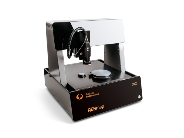
RESmap

Skip breadcrumb navigation Breadcrumb Freiberg Instruments Products Resistivity Mapping RESmap RESmap High-Precision Resistivity Mapping System for Accurate Material Analysis Interested? Get in touch! Contact now Product Sheet Skip menu Quick navigation Features Applications Specifications Technology Software Contact Fast and reliable resistivity mapping tool for highly doped samples Exceptional Repeatability (sigma < 0.15%) Advanced Stability Sensors Seamless Inline Integration and Effortless Calibration Materials The RESmap is specialized on highly doped materials Si SiC and more Features & Benefits Sigma < 0.15 % exceptional repeatability Resistivity 1–100 mOhm cm Throughput > 20 Wafers/hour ± 5 % accuracy with temperature correction ± 5 % accuracy with temperature correction Exceptional Repeatability Achieves ultra-high precision with a standard deviation of less than 0.15%, ensuring consistent and reliable results. Advanced Stability Sensors Features an integrated distance and temperature sensor, maintaining superior measurement accuracy and stability Seamless Inline Integration Available as a fully automated, compact sensor, ideal for smooth and efficient inline applications Effortless Calibration Enables easy and stable calibration using a dedicated sample set, reducing setup time and ensuring long-term reliability Contact free measurement and imaging of the resistivity High frequency eddy current sensing principle with integrated IR temperature sensor to correct for temperature variations of the sample Material form factor Flat or slightly curved wafers, boules, ingots slabs, blanks and thin films X-Y placement resolution ≥ 0.1 mm Edge exclusion 5 mm Reliability modular, compact bench top instrument design for high reliability and uptime > 99% Measurement time < 3s for the measurement and < 1s between measurements Measurement speed < 30s for a 200 mm wafer/ingot, 9 points Bull´s eye chart management for maximum accuracy and precision Measurement principle of eddy current sensor Applications High precision Resistivity Measurement Measuring resistivity in highly doped semiconductors is crucial for several reasons:Quality control and Doping density verification, Device performance prediction, Extraction of material… Learn more RESmap delivers unmatched repeatability, stability and accuracy – making it the trusted choice for precise resistivity mapping across a wide range of materials. Dr. Christian Hagendorf Key Account Manager Interested? Our experts are happy to assist you. Get in touch! Contact us now! Prepared for Automation different platforms available Measurement method conforms with SEMI MF673 Data and data validity checked using NIST standards Accuracy over calibration interval ±1% Integrated IR temperature sensor (±0.1°) to allow reporting resistivity at a standard temperature, different from the actual temperature of the sample Sample thickness correction for samples where the penetration depth of the high frequency signal is larger than the penetration depth Power requirements 100-250 VAC, 5 A Dimensions (w/h/d) 465 x 550 x 600 mm Software control standard PC with Window 10 or latest, 2 Ethernet ports Download Product Flyer PDF (167 KB) Technologies Minority carrier lifetime The measured effective lifetime is composed of the bulk lifetime and surface lifetime, which depends on the surface properties of a sample. Hence the surface has to be passivated, if you want… Learn more Photoconductivity When light of sufficient energy is absorbed by a semiconductor, the number of free electrons and holes changes and raises the electrical conductivity of the semiconductor. This increase is… Learn more Resistivity The electrical resistivity directly depends on the density of the semiconductor and is therefore a useful parameter to monitor doping profiles and homogeneity. The lifetime and diffusion length… Learn more Mobility The mobility is a quantity related to the drift velocity of electrons or holes in an applied electric field across a material. The mobility depends on different scattering processes that can… Learn more Diffusion length Learn more Defect properties The properties of a defect and its impact on the material quality can be described by three main parameters:defect concentration NT, capture cross sections for electrons and holes σn, σp,… Learn more Lifetime simulations From the simulated time dependent carrier concentrations the photoconductivity can be calculated using the mobility model of DORKEL and LETURCQ [2] . The minority carrier lifetime can be… Learn more Simulation of carrier profiles The measurement of thick samples as bricks leads to new questions and problems. One of these questions is how the carrier profiles that develops in a sample effect the lifetime measurements. To… Learn more Microwave detected photoconductivity (MDP) The novel method MDP is well suited for both, defect investigation by e.g. injection dependent minority carrier lifetime measurements, as well as mapping of wafers or even bricks for inline… Learn more Comparison to µ-PCD and QSSPC Besides MDP the two most important contact less lifetime measuring methods are QSSPC (quasi steady state photoconductivity) and µ-PCD (microwave detected photoconductive decay). Currently one… Learn more MD-PICTS MD-PICTS is a modification of MDP, where temperature dependent measurements of the defect part of the transient are accomplished. This allows for a spatially resolved defect characterization.… Learn more Penetration depth of different laser wavelength in silicon The microwave detected photoconductivity measures the photoconductivity after the irradiation of the sample with light. Usually the light should have an energy that is higher than the bandgap,… Learn more Materials Electrical properties and defects of a large variety of semiconductor materials, devices and dielectric materials can be investigated contact less and destruction with our advanced method MDP.… Learn more User-friendly and advanced operating software with Resistivity measurement recipes Export/import functions and raw data access Multi-level user account management Overview over all performed measurements Mapping options (line, cross, star, full map, topography, user defined pattern) Package of analysis functions; statistics, variance analysis, temperature correction functions and library Remote accessibility; Internet based based system allows remote operation and technical support from anywhere in the world Get in touch Do not hesitate to contact us – we are available to assist you with any inquiries or requests. Use our inquiry tool or reach out via email: sales @ freiberginstruments.com

Product

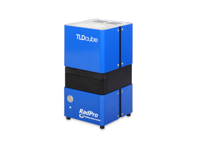
TLDcube

Skip breadcrumb navigation Breadcrumb Freiberg Instruments Products Luminescence Dating and Dosimetry TLDcube TLD cube A modern TLD reader by Freiberg Instruments Exclusively through RadPro International Contact for demo Product Sheet Skip menu Quick navigation Features Applications Specifications Software Contact Features & Benefits TLDcube is a small, lightweight and portable TLD Reader for measuring, analyzing and evaluating of thermoluminescent materials. The ceramic heater with defined nitrogen cooling in the rotating drawer accepts all standard TLD shapes Single element Measurement chamber (TL) End point temperature up to 600°C Photosensor (300 - 650 nm) Exchangeable detection filter Download Product Sheet PDF (292 KB) Applications Thermoluminescence (TL) Thermoluminescence (TL) is a backbone in radiation protection dosimetry with a long tradition and used for a wide range of dosimetric purposes, including accident dosimetry, retrospective… Learn more Neutron dosimetry Active dosimeters, like rem-mteters, superheated emulsions and electronic personal dosemeters can be used to measure neutron fields. But frequently passive dosemeters are used to determine… Learn more Food Irradiation Control Food stuff often is irradiated with ionizing radiation for sterilisation purposes. This requires the detection and estimates of the applied doses. The attached mineral dust or the food itself… Learn more Medical dosimetry Ionizing radiation from a large variety of isotopic sources, as well as accelerators, electron beams, etc. are increasingly used in radiotherapy. Clinical diagnostics employing ionizing radiation… Learn more Other applications: → Radiation protection → Personnel dosimetry → Environmental research → Experimental physics TLDcube – Exclusively through RadPro International This product is distributed by our trusted partner. Contact for demo Specifications Heater State-of-the-art ceramic contact heater with thermocouple Measurment chamber Sealed chamber with nitrogen circulation pump and cooling function Base plate Stainless steel, exchangeable Base plate (type) Chip 3.2 mm x 3.2 mm, Rod 1 mm x 6 mm, Disc Ø 4.5 mm, Multi-Purpose Ø 10 mm Powder dish Inner Ø 8 mm, outer Ø 10 mm Capacity Single element (one sample per load) Linear heating ramps Adjustable up to 20 K/s Heating program Multi-step program, adjustable temperatures ±1 K End point temperature up to 600°C Readout time Freely adjustable Accuracy ±1 % S.D. (for multiple readout) Stability Better than ±1% during 8 h operation Test light Stability < 0.5%, colour blue Detector Thermoelectric temperature stabilization Measurement range 7 decades Signal processing 24 bit, full digital evaluation system Neutral density filters Exchangeable Shielding and cooling gas Nitrogen, approx. 300 ml per measurement Software TLStudio - windows based software with full calibration and export functions Data output LAN to PC Power supply 100/240 V, 50-60 Hz Power consumption 200 VA Dimensions (W x D x H) 15 x 17 x 29 cm Weight ca. 5 kg Transport case 48 x 25 x 25 cm, 11 kg (incl. TLD Cube reader) All information are subject to technical changes without notice. Software TLStudio - Operating & Evaluation software User account management system, Transperent workflow, Professionally designed user interface, Intelligent parameter selection, Live data visualization, Easy programming of individual and… Learn more TLDcube – Exclusively through RadPro International This product is distributed by our trusted partner. Contact for demo

Product

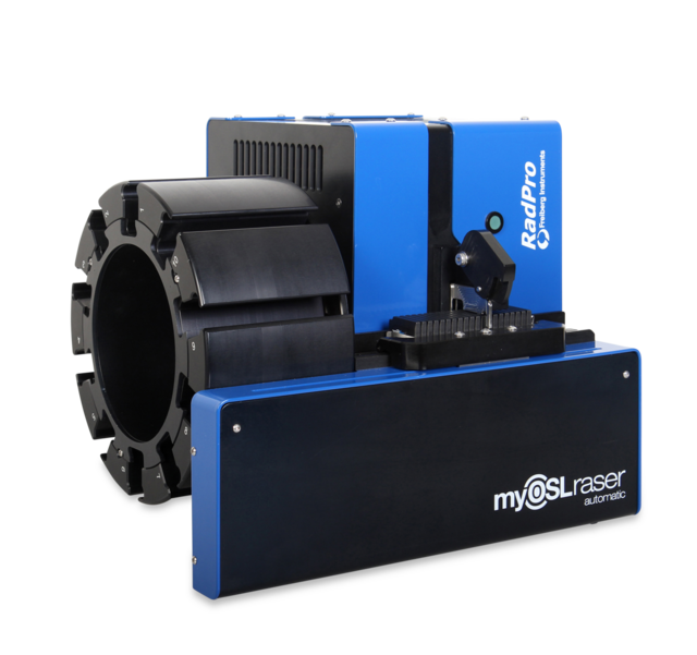
myOSLraser 2.0

Skip breadcrumb navigation Breadcrumb Freiberg Instruments Products Luminescence Dating and Dosimetry myOSLraser myOSLraser 2.0 myOSL raser 2.0 Most advanced OSL system for personal dosimetry Exclusively through RadPro International Contact for demo Product Sheet Skip menu Quick navigation Features Specifications Options Software Contact Features & Benefits The OSL reader myOSLraser 2.0 (reader + eraser) is an automatic device for evaluation of OSL dosimeters called "myOSL" dosimeters with a loading capacity of one dosimeter manual device for evaluation of its single OSL dosimeter called "myOSL" dosimeters. Equipped with a feeder it automatically processes up to 200 myOSL dosimeter per loading. The myOSLraser also includes an erasing unit (4 LEDs) which also provides the capability of erasing the residual signal from the OSL detectors in the same device. This function can be activated or deactivated if a second readout is requested according to an adjusted dose threshold. Up to 200 myOSL dosimeter per loading includes an erasing unit (4 LEDs) automatic drawer for single OSL dosimeters fast OSL read outs (few seconds) fast OSL read outs (few seconds) manual or automatic process of up to 200 OSL dosimeter manual system upgradeable to automatic system at any time remote control (IP device) easy operation erasing function selectable according to the last dose measurement self check diagnostic no consumables like gas myOSLraser 2.0 – Exclusively through RadPro International This product is distributed by our trusted partner. Contact for demo Technical specifications OSL reading YES Erasing function YES LED stimulation blue, 480nm Reading time per dosimeter <10s Processing speed per hour ca. 100/h including erasing ca. 200/h without erasing Test light stability better 1%/a Power supply voltage 100-240V, 50/60Hz Dimension 300 x 230 x 200 mm Weight 13 kg Download Product Sheet PDF (304 KB) Accessories & Options myOSL dosimeter holder Interested? Get in touch! Learn more myOSL blister holder Interested? Get in touch! Learn more Software OSLdosimetry OSLdosimetry is a user friendly operating software which allows OSL dose measurements as standard user or calibration and setting features for professionals (password protected). The… Learn more myOSLraser 2.0 – Exclusively through RadPro International This product is distributed by our trusted partner. Contact for demo