Found 271 results in 1 milliseconds.

Application

Contactless characterization of SiC, GaN and AlGaN

Contactless characterization of SiC, GaN and AlGaN Aim SiC, GaN and AlGaN belong to the class of wide band gap semiconductors and are applied especially in power electronics, optoelectronic devices and transistors such as HEMTs (high electron mobility transistor. The contactless optoelectronic characterization of wide band gap semiconductors and heterostructures under production conditions and in fields of R&D is often challenging. Solution SPV spectroscopy in the dc (Kelvin probe, measurement of the contact potential difference, DCPD) and ac (modulated) modes provides information about preferential directed charge separation in relation to electronic transitions and carrier dynamics [1]. The application of charge amplifiers allows for SPV measurements in dc and ac modes with the same electrode. Application example Figure 1 shows DCPD spectra of GaN, Al 0.25 Ga 0.75 N/GaN and 4h-SiC/GaN deposited onto sapphire wafers. Aside directions of charge separation and transition energies at band gaps, defect transitions can be distinguished. Signatures of slow processes can be discriminated in modulated SPV measurements (figure 2). References [1] Th. Dittrich, S. Fengler, “Surface photovoltage analysis of photoactive materials”, World Scientific, 2020. [2] Th. Dittrich, S. Fengler, N. Nickel, “Surface photovoltage spectroscopy over wide time domains for semiconductors with ultrawide bandgap: example of gallium oxide”, Phys. Stat. Sol. A 11 (2021) 2100176. Fig. 1: DCPD spectra of GaN (blue), Al0.26Ga0.74N / GaN (green) and 4h-SiC / GaN (red) epitaxial layers deposited on sapphire. Fig. 2: Modulated in-phase and phase-shifted by 90° SPV spectra of GaN (a), 4h-SiC / GaN (b) and Al0.26Ga0.74N / GaN (c). Related Solutions and Industries: Epitaxial Layers & Thin Films Matching Products SPS/SPV series HR-SPSmap with fixed energy excitation sources High-Resolution and Sensitive Surface Photovoltage Measurement Solutions Learn more SPS/SPV series HR-SPSmap with variable energy excitation source with a variable energy excitation source Learn more Get in touch Do not hesitate to contact us – we are available to assist you with any inquiries or requests. Use our inquiry tool or reach out via email: sales @ freiberginstruments.com

Application

Contactless detection of bulk polarization phenomena in semiconductors

Contactless detection of bulk polarization phenomena in semiconductors Aim Characterization of bulk polarization phenomena such as the bulk photo-voltaic effect (BPVE) in semiconductors requires the preparation of two electrical contacts on the sample, which inevitably introduces additional defects in the semiconductor-metal interface what is especially challenging for ultrawide bandgap semiconductors with high resistivity. Solution Surface photovoltage (SPV) spectroscopy using a Kelvin probe is used as a nondestructive, contactless method for characterizing the change of the contact potential difference (DCPD) in carbon doped GaN single crystals. By designing a unique setup capable of measuring DCPD up to ± 200 V, large photovoltages could be detected, without the need to deposit electrical contacts. Application example The band gap of GaN is 3.4 eV. As an example, figure 1 shows a spectrum of DCPD for a carbon doped GaN crystal (GaN:C). The corresponding SPV signal reached more than 13 V at 3 eV, i.e., under excitation of certain defect states, SPV signals were much larger than expected from the band gap (for more details see [1]). A change of the direction of DCPD and a signature in the derivative were found near the band gap. Under excitation with a laser diode (445 nm) at higher intensity, the maximum signal was obtained for GaN:C with a carbon concentration of 9×10 18 cm -3 and amounted to about 23 V, far exceeding the band gap (figure 2). Fig.1: Spectra of DCPD and its deriva-tive for a GaN:C crystal. SPV signals are much larger than the band gap for excita-tion in the defect range (data after [1]). Fig. 2: Time dependence of DCPD of a GaN:C crystal measured during illumination with a laser diode at 445 nm and after switching off illumination. References [1] Levine, I., et al. "Bulk photovoltaic effect in carbon-doped gallium nitride revealed by anomalous surface photovoltage spectroscopy." Phys. Rev. B 101 (2020) 245205. Related Solutions and Industries: Epitaxial Layers & Thin Films Matching Products SPS/SPV series HR-SPSmap with fixed energy excitation sources High-Resolution and Sensitive Surface Photovoltage Measurement Solutions Learn more SPS/SPV series HR-SPSmap with variable energy excitation source with a variable energy excitation source Learn more Get in touch Do not hesitate to contact us – we are available to assist you with any inquiries or requests. Use our inquiry tool or reach out via email: sales @ freiberginstruments.com

Industry

Crystal Growth and Processing

Crystal Growth and Processing Solutions for Unrivaled Precision in Crystal Orientation Enhancing Accuracy in Grinding and Sawing: Optimize your Crystal Processing Freiberg Instruments sets new standards in crystal growth and processing with state-of-the-art metrology solutions. Our advanced tools ensure precise alignment of high-mobility crystal directions with transistor channel orientations, enabling peak performance in semiconductor and material fabrication industries. Key Advantages Tailored to your workflow Every fab is unique, like a living organism. Our tools are meticulously designed to seamlessly integrate into your material workflows and data processing systems. Highest precision Our method stands unrivalled in combining precision, speed, and 3D crystal orientation. Leveraging our proprietary algorithms, we calculate the optimal cylinder and empower cost-efficient process tools with a single Ingot XRD solution. Comprehensive seed-to-wafer solution framework We provide tailored solutions for every stage of oriented crystal manufacturing, offering a wide range of customized options to meet market demands. Bring us your toughest process challenges – we're ready to deliver! Onsite service and training Reduce your total cost of ownership by participating in our on-site training program! We empower you to perform first- and second-line servicing on your tools, ensuring maximum uptime and full control over your process – no matter your location or access limitations. Precision in Every Step XRD series Explore more Ingot XRD Learn more Ingot XRD SiC Learn more Omega/Theta XRD Learn more Expertise in Materials Si SiC InP GaAs Ga₂O₃ Ge and more Future-Proof Your Manufacturing Process As industry demands evolve, so do our solutions. Freiberg Instruments remains at the forefront of innovation, helping clients optimize efficiency, investigate defects, and maintain a competitive edge in crystal growth and processing. Revolutionize your ingot grinding preparation with Ingot XRD 300 OD/Notch Get in touch Do not hesitate to contact us – we are available to assist you with any inquiries or requests. Use our inquiry tool or reach out via email: sales @ freiberginstruments.com Discover More Solutions Epitaxial Layers & Thin Films Learn more Photovoltaic Learn more Luminescence Dating and Dosimetry Learn more Research and Development Learn more

Application

Crystal Surface Orientation Mapping

Crystal Surface Orientation Mapping Surface mapping is key to identifying issues in crystal growth and manufacturing Precise Surface Orientation Mapping with Omega-Scan Even within a single crystal, slight variations in crystal orientation can occur across the surface, often due to internal strains from lattice defects. Similarly, well-grown thin films can display unique in-plane orientation distributions. Mapping such surfaces typically requires numerous measurements, and this is where the Omega-Scan method excels with its speed and efficiency. The image below illustrates an orientation map measured on a (Si, Ge) solid solution wafer, where the maximum orientation difference is just 0.03°. The concentric circles in the map correspond to the crystal’s growth rings, providing valuable insights into its structure. Related Technologies: Omega-scan , Theta-scan Related Solutions and Industries: Epitaxial Layers & Thin Films Matching Products XRD series Omega/Theta XRD for ultra-fast crystal orientation, crystal alignment in production, quality control, rocking curve measurements, material research and more Learn more XRD series XRDmap Pro Inline wafer orientation mapping truly fab compliant Learn more Get in touch Do not hesitate to contact us – we are available to assist you with any inquiries or requests. Use our inquiry tool or reach out via email: sales @ freiberginstruments.com

Application

Crystal quality

Measuring Crystal Quality Through XRD Reflection Analysis Assessing Crystal Quality via XRD Reflection Analysis Crystal quality cannot be directly measured, but several physical properties can be assessed and compared to standards for pure, homogeneous crystals. One such property is the half-width of an X-ray diffraction (XRD) reflection. The regularity of the crystalline lattice defines its quality. Imperfections such as defects, dislocations, and contaminants are inherent in every lattice. Additional discontinuities, like grain boundaries and cracks, also exist. These imperfections introduce local strain within the surrounding lattice, which can be detected by recording the rocking curve of an X-ray reflection. By analyzing the geometric properties of the incident beam and the resulting rocking curve half-width, the surface quality of the crystal can be effectively characterized. Related Technologies: Omega-scan Matching Products XRD series SDCOM Ultra-fast, top surface measuring crystal orientation in a compact package Learn more XRD series Omega/Theta XRD for ultra-fast crystal orientation, crystal alignment in production, quality control, rocking curve measurements, material research and more Learn more Get in touch Do not hesitate to contact us – we are available to assist you with any inquiries or requests. Use our inquiry tool or reach out via email: sales @ freiberginstruments.com

Page

Customization

Customization Tailored Measurement Solutions for Unique Challenges Solutions Built for Your Needs At Freiberg Instruments, we understand that standard solutions may not always fit your specific requirements. That’s why we offer customized adaptations and developments, ensuring that our instruments align perfectly with your production workflows, environments, and research goals. Contact Us Our Customization Services We work closely with you to modify existing products or develop entirely new solutions tailored to your needs. Our customization services include: Instrumentation Modifications We tailor metrology and automation solutions to meet your unique needs, delivering precision, efficiency, and seamless integration. Software Adaptations Custom interfaces, automation scripts, and advanced data processing tailored to your specific analysis and reporting requirements. Precision Measurement Solutions Designing innovative measurement techniques and advanced quality control systems tailored for specialized applications. Integration with Existing Systems Seamless incorporation of our instruments into your current infrastructure, ensuring smooth operation within your production line or laboratory setup. Our Process: From Concept to Implementation Understanding Your Needs: We start by assessing your requirements and production environment to understand the challenges you face. Designing the Solution: Our team collaborates with you to design modifications or new devices that match your application needs, including tailored hardware and software adjustments. Integration and Testing: We integrate the customized solution into your workflow, conduct rigorous testing, and ensure everything operates smoothly. Deployment & Support: After successful testing, we assist with implementation, provide documentation, and offer ongoing support to maintain performance. Why Choose Freiberg Instruments for Customization? Expertise in Precision Instrumentation With more than 20 years of expertise in developing and enhancing cutting-edge measurement solutions. Close Collaboration We work hand in hand with our customers to develop solutions that truly meet their needs. Agility & Innovation Our team is equipped to adapt quickly and develop innovative approaches to complex measurement challenges. Reliable Support Continuous assistance from consultation to post-installation ensures a smooth experience. Frequently asked questions What types of customizations does Freiberg Instruments offer? We provide metrology, automation, hardware modifications, software adaptations, specialized measurement solutions, and seamless system integration to meet your unique needs. What is the typical timeline for a customization project? The timeline varies depending on complexity, but a typical customization project follows a structured process from consultation to deployment, ensuring efficiency without compromising quality. Can Freiberg Instruments integrate customized solutions into existing systems? Yes, we ensure that our instruments seamlessly integrate with your current infrastructure to enhance workflow efficiency and productivity. What kind of support is available after customization? We offer comprehensive documentation, training, and ongoing technical support to ensure the continued performance of your customized solution. How can I get started with a customization request? Simply contact us with your requirements, and our team will guide you through the consultation and development process to create a solution that fits your needs. Your challenges inspire our innovation. We tailor metrology and automation solutions to meet your unique needs, delivering precision, efficiency, and seamless integration. Burkhard Winkler Senior Sales Manager SEMI & Automation Tailored Solutions, Built Together Get in touch with us today to discuss your customization needs and discover how our precision-engineered measurement solutions can optimize your processes. Use our inquiry tool or reach out via email: sales @ freiberginstruments.com Discover more Automation Learn more Research and Development Learn more Training and Application Expertise Learn more Technical Support Learn more
Product

DDCOM

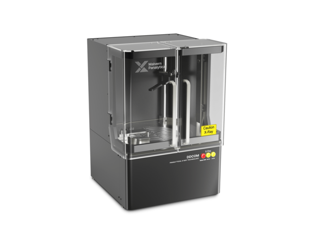
Skip breadcrumb navigation Breadcrumb Freiberg Instruments Products X-ray Diffraction DDCOM DDCOM Ultra-fast, bottom surface measuring crystal orientation in a compact package Exclusively through Malvern Panalytical Contact for demo Product Sheet Skip menu Quick navigation Features Applications Specifications Technology Options Software Contact Materials With DDCOM, a wide variety of materials can be precisely analyzed. Thanks to their flexibility and performance, our systems meet even the most demanding requirements. Ag Al₂O₃ (sapphire) AlSb Au CdTe GaAs GaN GaP GaPO₄ GaSb Ge InAs InP InSb La₃Ga₅SiO₁₄ LaTiO₃ LiF LiNbO₃ Mg₂SiO₄ MgAl₂O₄ MgF₂ MgO NdGaO₃ Ni PbS PbTe Pt Si SiC 2H SiC 4H SiC 6H SiC 15R SiC₃C SiO₂ (quartz) SnTe SrLaAlO₄ SrTiO₃ TiO₂ ZnO ZnTe and more Features & Benefits Ultra-fast Omega-scan approach 200 times faster than Theta-scan method Automatic evaluation of the complete lattice orientation in 3D Determination of entire crystal orientation within 5 seconds Efficient workflows for quality control For standard research and industrial workflows Azimuthal setting and marking of crystal orientation Preprogrammed cubic crystal parameters State-of-the-art and convenient software High precision, i.e up to (1/100)° Compact, user friendly and cost effective Easily movable and lightweight desktop design Convenient sample handling and easy to operate Low energy consumption and operating costs due to air cooled X-ray tube (no water cooling required) Control of cutting, grinding and lapping Complete lattice orientation of single crystals Suitable for a unique variety of materials in a large range of size and weight, such as: Wafers from 2-12” and Ingots up to 20kg Highlights Determination of the complete lattice orientation of single crystals Ultra-fast crystal orientation measurement using the Omega-scan method Determination of the arbitrary unknown orientation of cubic crystals Designed especially for azimuthal setting and marking of lattice directions Air cooled X-ray tube, no water cooling required Appropriate for research and production quality control Omega-scan diagram (Quartz) easy sample allignment Omega-scan method: All desired crystal orientation parameters are captured in one rotation within 5 seconds. Applications Samples with a wide variety of geometry & size The industrial synthesis of single crystals begins with large, heavy boules and is processed down to smaller forms, such as wafers or blanks. In experimental growth, tiny cylinders are produced.… Learn more Marking and measuring of in-plane directions The Omega Scan provides a complete crystal orientation in a single measurement, allowing for the direct identification of in-plane directions. This feature is particularly useful for marking… Learn more DDCOM – Exclusively through Malvern Panalytical This product is distributed by our trusted partner. Contact for demo Technical specifications X-ray source 30 W air-cooled X-ray tube, Cu anode Detectors Two scintillation counters Sample holder Precise turntable, setting accuracy 0.01°, tools for defined sample positioning and marking Dimensions 600 mm × 600 mm × 850 mm Weight 80 kg Power supply 100-230 V, 100 W, single phase Room temperature ≤ 30° C Technologies Omega-scan Ultra-Fast Orientation Measurement for Single Crystals Learn more Theta-scan Precision X-ray Method for Single Crystal Orientation Learn more Accessories & Options Device for mapping of wafers (maximum diameter 225 mm) Device for automatic loading from cassettes Software XRDStudio Multiple Operating ModesOperator Mode: Designed for fixed measurement parameters, ensuring a safe and streamlined workflow. Administrator Mode: Allows for the creation and modification of… Learn more DDCOM – Exclusively through Malvern Panalytical This product is distributed by our trusted partner. Contact for demo

Product

DPM100

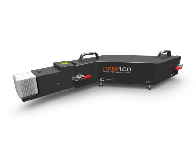
Skip breadcrumb navigation Breadcrumb Freiberg Instruments Products Double Prism Monochromator DPM100 DPM100 Wide range double prism monochromator Interested? Get in touch! Contact now Product Sheet Skip menu Quick navigation Features Technology Contact Enables the adjustment of the wavelength over a wide spectral range without any discontinuities Extremely wide spectral range (0.4–7.3 eV/ 170 - 3100 nm) Spectral resolution: 2 meV – 100 meV (depending on wavelength and slit width) Excellent stray light suppression Materials The DPM100 can be used for all kinds of materials Si SiC Ge GaAs Ga₂O₃ InP Diamond and more Features & Benefits 0.4–7.3 eV Spectral range >10⁸ Stray light suppression 3 mm Spot diameter 2–100 meV Spectral resolution 2–100 meV Spectral resolution Interested? Our experts are happy to assist you. Get in touch! Contact us now! Technologies Electrical and optical characterization using surface photovoltage spe Photocarrier generation and separation mechanisms, Minority carrier lifetime measurement/Diffusion length calculations, Trapped carrier dynamics, time resolved, Surface Photovoltage… Learn more SPV signal analysis: fits and simulations We are currently developing simulation tools to enable first principle calculations of the electronic structure in a given photoactive material or material combination, based on solid-state… Learn more Comparison between MPD and SPV techniques MDP (microwave detected photoconductivity): sensitive to moving photogenerated charge carriers (bulk property), SPV (surface photovoltage): sensitive to surface AND bulk properties with respect… Learn more Static, transient or modulated light excitation pro and con The time-resolved or frequency-modulated, surface photovoltage spectroscopy (SPS) is based on a time-resolved/frequency modulated measurement of the spectral dependence of the surface… Learn more SPV-Picts SPV temperature dependence measurements Use this option to make SPV measurements at different temperatures between room temperature and 200°C. Temperature-dependent SPV measurements can be applied to measure activation energies or to… Learn more Materials Any photoactive material from raw material to finished device:From powder-based samples over wafers to boules or ingots. From 10 x 10 mm2 and up to 300 mm diameter, From titanium dioxide over… Learn more Get in touch Do not hesitate to contact us – we are available to assist you with any inquiries or requests. Use our inquiry tool or reach out via email: sales @ freiberginstruments.com

Technology

Defect properties

Defect properties For the efficiency of solar cells the properties of a defect and its impact on the material quality are of great importance. Defect properties The properties of a defect and its impact on the material quality can be described by three main parameters: defect concentration N T capture cross sections for electrons and holes σ n , σ p activation energy E T All these properties are part of the simulation models we use and they can be measured beside the defect concentration with the temperature dependent method MD-PICTS . Fig. 1: Energy scheme of a defect and its important parameters Matching Products MDP series MDPmap Precision Lifetime Charachterization with Exceptional Sensitivity Learn more MDP series MDPspot Quick and Simple Lifetime Measurement Made Easy Learn more MDP series MDpicts pro High-Resolution, Temperature-Dependent Lifetime Measurement System for Precise Material Characterization Learn more MDP series MDPpro 850+ Advanced Solution for Quality Control of Monocrystalline Silicon Ingots, Bricks, and Wafers Learn more MDP series MDPlinescan Versatile OEM Unit for Lifetime Measurements on Silicon Samples, from Bricks to Processed Wafers Learn more MDP series MDpicts Temperature-Dependent Lifetime Measurement System for Advanced Material Analysis Learn more RES series RESmap High-Precision Resistivity Mapping System for Accurate Material Analysis Learn more Get in touch Do not hesitate to contact us – we are available to assist you with any inquiries or requests. Use our inquiry tool or reach out via email: sales @ freiberginstruments.com

Application

Defects and charge dynamics in 3C- and 4H-SiC investigated by surface

Defects and charge dynamics in 3C- and 4H-SiC investigated by surface Photoelectrochemical (PEC) and photocatalytic (PC) water splitting for hydrogen and/or oxygen generation is leading the way not only to green hydrogen production, but also to oxygen generators working solely on water basis. The quest for stable materials that can work with solar light as a basis has identified two superior photoactive material candidates, namely silicon carbide (SiC) and copper oxide (Cu 2 O) materials, based on a number of criteria such as cost, abundancy, toxicity and sustainability. The optimum photoelectrical conversion electrode is often a very complex system, where the focus is on a very fast separation of the generated charges in order to increase the current densities out of the cells. The charge dynamics of the complex systems, be it on SiC, Cu 2 O or any other photoactive material, can best be measured using time resolved surface photovoltage spectroscopy/measurements. The SPVcheck tool is again the optimum choice, because it can be configured in a flexible way concerning sample geometry and energy selection range. A 2 UV/VIS light source (480 and 660 nm) approach can give a lot information about the charge dynamics in the photoelectrode and can be used to check the quality of the photoelectrical conversion electrodes in a high-volume production setup. 4H-SiC under UV light 3C-SiC under normal light (solar spectrum) Related Solutions and Industries: Epitaxial Layers & Thin Films Matching Products SPS/SPV series HR-SPSmap with fixed energy excitation sources High-Resolution and Sensitive Surface Photovoltage Measurement Solutions Learn more SPS/SPV series HR-SPSmap with variable energy excitation source with a variable energy excitation source Learn more Get in touch Do not hesitate to contact us – we are available to assist you with any inquiries or requests. Use our inquiry tool or reach out via email: sales @ freiberginstruments.com