Found 271 results in 1 milliseconds.

Technology

Static, transient or modulated light excitation pro and con

Static, transient or modulated light excitation pro and con The time-resolved or frequency-modulated, surface photovoltage spectroscopy (SPS) is based on a time-resolved/frequency modulated measurement of the spectral dependence of the surface photovoltage (SPV). It is a powerful non-destructive and contactless characterization method. It is mainly used to study the electronic transitions and optical properties of bulk materials, thin films and heterostructures. High sensitivity and the possibility of room temperature measurements are the key advantages of the SPV method. Another advantage is that there is no need for the preparation of a front contact on the investigated sample. In general, there is no need for preparing the sample for the measurement, allowing to investigate the sample under operation/process conditions in a wide temperature range under different atmospheric conditions. The information depth and thereby the possibility to extract bulk properties is limited by the lights penetration depth and the diffusion length. In comparison to other spectroscopic methods, such as but not limited to optical transmission, deep level transient spectroscopy, photoluminescence or Raman spectroscopy, the time-resolved/frequency modulated SPS or SPV (fixed wavelength) method is fast and uncomplicated and is thus an ideal tool for production floor decisions of sample quality. We distinguish between 3 different excitation modes, but common to all of them is that the relaxation aspect of states in the samples are resolved under ideal conditions. A static SPV measurement is sensitive to any fast or slow process that lead to the separation of photogenerated carriers in space. The sample is illuminated until a saturation of the SPV signal is observed, after which the light is switched of. Measuring 1) the static SPV signal and 2) the time-resolved relaxation time gives a lot of useful information about the state of the material. A SPV measurement that is performed under modulated illumination in a fixed capacitor arrangement is very sensitive to small changes in the SPV signal. And, only those SPV signals, which can follow the modulation frequency are contributing to the measured signal. The response of processes with relaxation times much longer than the modulation period are simply filtered out. The most sensitive SPV measurement that can be made is a transient measurement, where illumination pulse of different pulse width are followed by a time dependent measurement of the decay of the SPV signal – in this way charge separation distances in the nanometre range can be investigated. This is particular important for surface or tunnelling dominated processes in the material. Matching Products SPS/SPV series HR-SPSmap with fixed energy excitation sources High-Resolution and Sensitive Surface Photovoltage Measurement Solutions Learn more SPS/SPV series HR-SPSmap with variable energy excitation source with a variable energy excitation source Learn more DPM series DPM100 Wide range double prism monochromator Learn more Get in touch Do not hesitate to contact us – we are available to assist you with any inquiries or requests. Use our inquiry tool or reach out via email: sales @ freiberginstruments.com
Technology

Comparison between MPD and SPV techniques

Comparison between MPD and SPV techniques MDP (microwave detected photoconductivity): sensitive to moving photogenerated charge carriers (bulk property) SPV (surface photovoltage): sensitive to surface AND bulk properties with respect to ANY photogenerated charge carriers separated in space (moving or trapped) The MDP method does only apply to moderately doped semiconductors or close to perfect optical crystals The SPV method apply to any photoactive materials allowing for charge separation in space (semiconductors, multilayer and multijunction structures, molecular layers, powders) The MDP method can be modelled as a time dependent resistance measurement (DC), t MDP The SPV method can be modelled as a frequency and time dependent capacitance measurement (DC/modulation), t SPV For a non-ideal semiconductor (with defects), there can be a huge difference between the two methods, both methods provide complementary information about bulk and surface properties Matching Products SPS/SPV series HR-SPSmap with fixed energy excitation sources High-Resolution and Sensitive Surface Photovoltage Measurement Solutions Learn more SPS/SPV series HR-SPSmap with variable energy excitation source with a variable energy excitation source Learn more DPM series DPM100 Wide range double prism monochromator Learn more Get in touch Do not hesitate to contact us – we are available to assist you with any inquiries or requests. Use our inquiry tool or reach out via email: sales @ freiberginstruments.com

Technology

SPV signal analysis: fits and simulations

SPV signal analysis: fits and simulations Charge dynamic simulations in photoactive materials, incl. heterojunction photoactive materials. We are currently developing simulation tools to enable first principle calculations of the electronic structure in a given photoactive material or material combination, based on solid-state physics. The SPS/SPV simulation tool enables users of any SPS/SPV equipment to verify their measurements against simulated scenarios. Thereby for instance reducing development time for new materials research and/or testing the tolerances of a given photoactive material configuration. All transient responses can be fitted between 10 ns and 100 ms using the build-in stretched exponentials multi-parameter fit function with three basic parameters; t I , β i and A i , where t is the transient time constant, β is the stretching factor to the exponential function and A is the signal amplitude. The multi-parameter i can in most cases be limited to 2 (i.e. i = 1,2), 5 is rare, but sometime needed for complex structures. In principle, fitting with i = 1,….,12 is possible. Figure 1 shows an example using SPV for the radial characterization of shallow defects close to the conduction band in a float zone silicon wafer using a fit function consisting of the sum of 5 stretched exponential functions. Matching Products SPS/SPV series HR-SPSmap with fixed energy excitation sources High-Resolution and Sensitive Surface Photovoltage Measurement Solutions Learn more SPS/SPV series HR-SPSmap with variable energy excitation source with a variable energy excitation source Learn more DPM series DPM100 Wide range double prism monochromator Learn more Get in touch Do not hesitate to contact us – we are available to assist you with any inquiries or requests. Use our inquiry tool or reach out via email: sales @ freiberginstruments.com

Technology

Electrical and optical characterization using surface photovoltage spe

Electrical and optical characterization using SPV/Kelvin Photocarrier generation and separation mechanisms Minority carrier lifetime measurement/Diffusion length calculations Trapped carrier dynamics, time resolved Surface Photovoltage measurements Figure 1 shows an example using SPV for the characterization of the polishing process on the double-side polished high-resistivity float zone silicon wafer. The red areas in the plots clearly show that the CMP polishing process is not optimal and even signatures of a handling tool are clearly visible in the plots (left below). Fig. 1: Using SPV for the characterization of the polishing process Matching Products SPS/SPV series HR-SPSmap with fixed energy excitation sources High-Resolution and Sensitive Surface Photovoltage Measurement Solutions Learn more SPS/SPV series HR-SPSmap with variable energy excitation source with a variable energy excitation source Learn more DPM series DPM100 Wide range double prism monochromator Learn more Get in touch Do not hesitate to contact us – we are available to assist you with any inquiries or requests. Use our inquiry tool or reach out via email: sales @ freiberginstruments.com

Page

Publications

Publications for HS-SPS Dittrich, T. and Fengler, S. (2025). Surface Photovoltage Spectroscopy of Ultrawide Bandgap Materials. Phys. Status Solidi RRL 2400384. https://doi.org/10.1002/pssr.202400384 Dittrich, Thomas & Fengler, Steffen & Franke, Michael. (2024). Mirrorless fused silica based double-prism monochromator for continuous measurements from the near infrared to deep ultraviolet. Applied Optics. 63. 6880-6886. 10.1364/AO.529366. Dittrich, Thomas. (2022). Transient surface photovoltage spectroscopy of diamond. AIP Advances. 12. 065206. 10.1063/5.0089398.

Page

Software

HR-SPS Software Software - SPS Studio Learn more

Page

Technology

HR-SPS Technology Electrical and optical characterization using surface photovoltage spe Photocarrier generation and separation mechanisms, Minority carrier lifetime measurement/Diffusion length calculations, Trapped carrier dynamics, time resolved, Surface Photovoltage… Learn more SPV signal analysis: fits and simulations We are currently developing simulation tools to enable first principle calculations of the electronic structure in a given photoactive material or material combination, based on solid-state… Learn more Comparison between MPD and SPV techniques MDP (microwave detected photoconductivity): sensitive to moving photogenerated charge carriers (bulk property), SPV (surface photovoltage): sensitive to surface AND bulk properties with respect… Learn more Static, transient or modulated light excitation pro and con The time-resolved or frequency-modulated, surface photovoltage spectroscopy (SPS) is based on a time-resolved/frequency modulated measurement of the spectral dependence of the surface… Learn more SPV-Picts SPV temperature dependence measurements Use this option to make SPV measurements at different temperatures between room temperature and 200°C. Temperature-dependent SPV measurements can be applied to measure activation energies or to… Learn more Materials Any photoactive material from raw material to finished device:From powder-based samples over wafers to boules or ingots. From 10 x 10 mm2 and up to 300 mm diameter, From titanium dioxide over… Learn more

Page

Applications

SPS/SPV Applications Silicon photovoltaic – Wafer check after diamond wire sawing Learn more Contactless detection of bulk polarization phenomena in semiconductors Learn more Electronic transitions in diamond Learn more Characterization of Ga2O3 Learn more Investigation of photocatalytic materials (BiVO4) Learn more Study and monitoring of photocatalytic materials (TiO2) Learn more Contactless characterization of SiC, GaN and AlGaN Learn more Defects in 4H-SiC Learn more Defects and charge dynamics in 3C- and 4H-SiC investigated by surface Learn more

Product

HR-SPSmap with variable energy excitation source

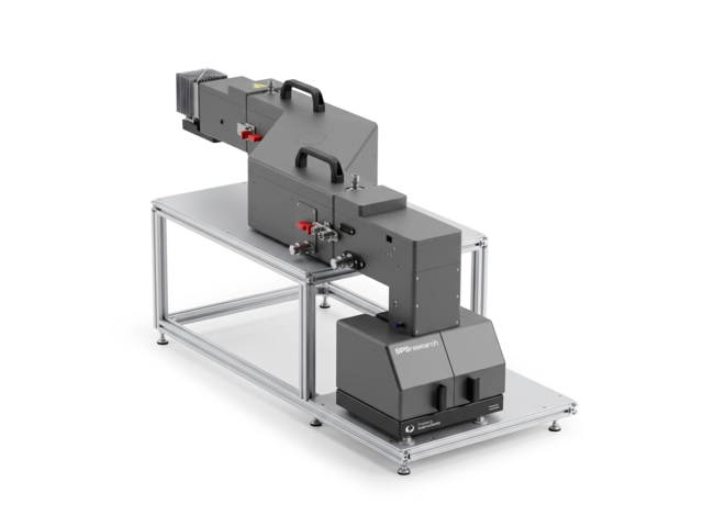
Skip breadcrumb navigation Breadcrumb Freiberg Instruments Products Surface Photovoltage Spectroscopy HR-SPSmap with variable energy excitation source HR-SPSmap with a variable energy excitation source Interested? Get in touch! Contact now Product Sheet Skip menu Quick navigation Features Applications Specifications Technology Options Contact Features & Benefits Sensitivity : μV sensitivity and more than 7 orders of magnitude signal height resolution Measurement speed : < 5 minutes per point for a 150 mm wafer with 1 mm resolution Time resolution : 10 ns up to 100 ms Optical head : laser driven light source with adjustable intensity and wavelength output between 200 and 3000 nm light. Spectral width < 10 nm. Reliability : Bench top instrument with build in monochromator for high reliability and uptime > 99% Customizable Mapping System for R&D Needs Flexible Mapping Tool for R&D The HR-SPSmap product with a variable energy excitation source is built on the same robust foundation as the fixed-excitation HR-SPSmap system. This compact, benchtop, contactless electrical characterization tool is designed for offline production control and research and development applications. It provides precise surface photovoltage (SPV) measurements across a wide injection range, supporting both steady-state and short-pulse excitation. Additionally, it offers continuous wavelength sweeps for true spectroscopy measurements, enabling reliable characterization of any photoactive sample. Versatile and Automated Adaptability The HR-SPSmap system is engineered for flexibility and efficiency. Automated sample recognition and parameter configuration allow seamless adaptation to a broad range of samples, including epitaxial layers and wafers processed at various stages, from raw material to fully finished devices. Whether for R&D innovation or stringent production monitoring, the HR-SPSmap with variable energy excitation delivers unmatched precision and versatility, setting a new standard in electrical characterization solutions. Applications Defects and charge dynamics in 3C- and 4H-SiC investigated by surface Photoelectrochemical (PEC) and photocatalytic (PC) water splitting for hydrogen and/or oxygen generation is leading the way not only to green hydrogen production, but also to oxygen generators… Learn more Defects in 4H-SiC Silicon carbide (SiC) high power, high voltage semiconductor devices lead the way not only for superfast chargers and on-board chargers for electrical vehicles (EV), but also power drive trains… Learn more Contactless characterization of SiC, GaN and AlGaN Aim SiC, GaN and AlGaN belong to the class of wide band gap semiconductors and are applied especially in power electronics, optoelectronic devices and transistors such as HEMTs (high electron… Learn more Study and monitoring of photocatalytic materials (TiO2) Aim Photocatalytic materials such as TiO2 are of great interest, for example, for cleaning of industrial wastewater and for water splitting. The identification of directed charge transfer is… Learn more Investigation of photocatalytic materials (BiVO4) Aim Photocatalytic materials such as BiVO4 are of great interest, for example, for water splitting. Electronic defect states and surface passivation are important limiting factors. Photocatalytic… Learn more Silicon photovoltaic – Wafer check after diamond wire sawing Diamond wire sawing (DWS) is an established technology for wafering semiconductor ingots, as it has many advantages over other technologies, such as of slurry cutting. Some of these advantages… Learn more Characterization of Ga2O3 Aim Ga2O3 is an ultra-wide band gap semiconductor with a great application potential. The contactless characterization of defect related transitions with high sensitivity is still… Learn more Electronic transitions in diamond Aim For further development of optoelectronic devices and other applications based on diamond and nanodiamond, contactless characterization of electronic defect states and electronic transitions… Learn more Contactless detection of bulk polarization phenomena in semiconductors [1] Levine, I. et al. "Bulk photovoltaic effect in carbon-doped gallium nitride revealed by anomalous surface photovoltage spectroscopy." Phys. Rev. B 101 (2020) 245205. Learn more Interested? Our experts are happy to assist you. Get in touch! Contact us now! Technical specifications sample size powder samples and up to 200 mm diameter excitation laser driven light source material any photoactive material (contact us for consultation on your material) measureable time-resolved and phase modulated surface photovoltage measurements dimensions 680 x 680 x 680 mm, weight: app. 100 kg power 100 - 250V, 50/60 Hz, 5 A Technologies Electrical and optical characterization using surface photovoltage spe Photocarrier generation and separation mechanisms, Minority carrier lifetime measurement/Diffusion length calculations, Trapped carrier dynamics, time resolved, Surface Photovoltage… Learn more SPV signal analysis: fits and simulations We are currently developing simulation tools to enable first principle calculations of the electronic structure in a given photoactive material or material combination, based on solid-state… Learn more Comparison between MPD and SPV techniques MDP (microwave detected photoconductivity): sensitive to moving photogenerated charge carriers (bulk property), SPV (surface photovoltage): sensitive to surface AND bulk properties with respect… Learn more Static, transient or modulated light excitation pro and con The time-resolved or frequency-modulated, surface photovoltage spectroscopy (SPS) is based on a time-resolved/frequency modulated measurement of the spectral dependence of the surface… Learn more SPV-Picts SPV temperature dependence measurements Use this option to make SPV measurements at different temperatures between room temperature and 200°C. Temperature-dependent SPV measurements can be applied to measure activation energies or to… Learn more Materials Any photoactive material from raw material to finished device:From powder-based samples over wafers to boules or ingots. From 10 x 10 mm2 and up to 300 mm diameter, From titanium dioxide over… Learn more Accessories & Options Our devices offer versatile configuration options to meet specific requirements effectively. Each model can be customized to ensure maximum flexibility and efficiency. Contact for more information Pulse width and height modulation Integrated heating stage (20–250 °C) Spot size variation Bias light Resistivity measurement (wafers) Reference wafer (Si) Get in touch Do not hesitate to contact us – we are available to assist you with any inquiries or requests. Use our inquiry tool or reach out via email: sales @ freiberginstruments.com

Product

HR-SPSmap with fixed energy excitation sources

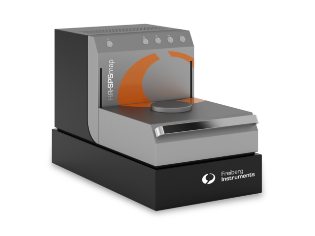
Skip breadcrumb navigation Breadcrumb Freiberg Instruments Products Surface Photovoltage Spectroscopy HR-SPSmap with fixed energy excitation sources HR-SPSmap High-Resolution and Sensitive Surface Photovoltage Measurement Solutions Interested? Get in touch! Contact now Product Sheet Skip menu Quick navigation Features Applications Specifications Technology Options Contact Enables advanced material research for thin layers and surfaces: destruction free, flexible and fast Highly sensitive due to an advanced electronic detection system Customized lasers and optics for up to 4 different wavelengths Investigation of charge separation processes and electronic transitions (defects) Materials Si SiC Ge GaAs Ga₂O₃ InP Diamond and more Features & Benefits 355–1550 nm Available wavelengths 10 ns Time resolution 0.1 mm Spatial resolution < 5 min Throughput for 8’’ wafer < 5 min Throughput for 8’’ wafer Sensitivity: sub-mV sensitivity and more than 3 orders of magnitude signal height resolution Measurement speed: < 5 minutes for a 150 mm wafer with 1 mm resolution Time resolution: 10 ns up to 100 ms Optical head: Up to 4 light sources integrated into the optical head or fixture for mounting of external lasers – build-in suppression of stray light Reliability: modular and compact bench top instrument for high reliability and uptime > 99% Flexible Mapping Tool for R&D and Production Monitoring The HR-SPSmap product platform builds on the proven foundation of the widely acclaimed MDPmap series. This compact, benchtop, contactless electrical characterization tool is specifically designed for offline production control and research and development applications. It measures surface photovoltage (SPV) across a wide injection range, accommodating both steady-state and short-pulse excitation. With automated sample recognition and parameter setup, it effortlessly adapts to a diverse range of samples, including epitaxial layers and wafers at various stages of processing, from as-grown material to fully fabricated devices. Exceptional Flexibility and Advanced Features One of the standout advantages of the HR-SPSmap is its exceptional flexibility. Equipped with fixed-energy excitation sources, the system supports the integration of up to four lasers within the measurement head. This capability facilitates injection-level-dependent SPV measurements across a broad range, from very low to high injection levels, and enables depth profiling using different laser wavelengths. The system also includes a bias light feature for enhanced measurement options. In addition, the HR-SPSmap supports custom calculations and mapping configurations, along with the ability to export primary data for detailed external analysis. For standard metrology tasks, the platform offers a predefined recipe system, allowing routine measurements to be completed with a single button press. Unlock Precision and Adaptability With its advanced capabilities and user-friendly design, the HR-SPS is the ideal solution for researchers and production teams seeking high-precision surface photovoltage measurements. Whether for R&D innovation or reliable production monitoring, this platform redefines flexibility and efficiency in electrical characterization. Applications Defects and charge dynamics in 3C- and 4H-SiC investigated by surface Photoelectrochemical (PEC) and photocatalytic (PC) water splitting for hydrogen and/or oxygen generation is leading the way not only to green hydrogen production, but also to oxygen generators… Learn more Defects in 4H-SiC Silicon carbide (SiC) high power, high voltage semiconductor devices lead the way not only for superfast chargers and on-board chargers for electrical vehicles (EV), but also power drive trains… Learn more Contactless characterization of SiC, GaN and AlGaN Aim SiC, GaN and AlGaN belong to the class of wide band gap semiconductors and are applied especially in power electronics, optoelectronic devices and transistors such as HEMTs (high electron… Learn more Study and monitoring of photocatalytic materials (TiO2) Aim Photocatalytic materials such as TiO2 are of great interest, for example, for cleaning of industrial wastewater and for water splitting. The identification of directed charge transfer is… Learn more Investigation of photocatalytic materials (BiVO4) Aim Photocatalytic materials such as BiVO4 are of great interest, for example, for water splitting. Electronic defect states and surface passivation are important limiting factors. Photocatalytic… Learn more Silicon photovoltaic – Wafer check after diamond wire sawing Diamond wire sawing (DWS) is an established technology for wafering semiconductor ingots, as it has many advantages over other technologies, such as of slurry cutting. Some of these advantages… Learn more Characterization of Ga2O3 Aim Ga2O3 is an ultra-wide band gap semiconductor with a great application potential. The contactless characterization of defect related transitions with high sensitivity is still… Learn more Electronic transitions in diamond Aim For further development of optoelectronic devices and other applications based on diamond and nanodiamond, contactless characterization of electronic defect states and electronic transitions… Learn more Contactless detection of bulk polarization phenomena in semiconductors [1] Levine, I. et al. "Bulk photovoltaic effect in carbon-doped gallium nitride revealed by anomalous surface photovoltage spectroscopy." Phys. Rev. B 101 (2020) 245205. Learn more Interested? Our experts are happy to assist you. Get in touch! Contact us now! Technical specifications sample size powder samples up to 300 mm diameter excitation select up to four different wavelengths from 337 nm up to 1550 nm (default 980 nm) material any photoactive material (contact us for consultation on your material) measureable time-resolved surface photovoltage measurements dimensions 680 x 380 x 450 mm, weight: app. 65 kg power 100 - 250V, 50/60 Hz, 5 A resolution 100 µm Technologies Electrical and optical characterization using surface photovoltage spe Photocarrier generation and separation mechanisms, Minority carrier lifetime measurement/Diffusion length calculations, Trapped carrier dynamics, time resolved, Surface Photovoltage… Learn more SPV signal analysis: fits and simulations We are currently developing simulation tools to enable first principle calculations of the electronic structure in a given photoactive material or material combination, based on solid-state… Learn more Comparison between MPD and SPV techniques MDP (microwave detected photoconductivity): sensitive to moving photogenerated charge carriers (bulk property), SPV (surface photovoltage): sensitive to surface AND bulk properties with respect… Learn more Static, transient or modulated light excitation pro and con The time-resolved or frequency-modulated, surface photovoltage spectroscopy (SPS) is based on a time-resolved/frequency modulated measurement of the spectral dependence of the surface… Learn more SPV-Picts SPV temperature dependence measurements Use this option to make SPV measurements at different temperatures between room temperature and 200°C. Temperature-dependent SPV measurements can be applied to measure activation energies or to… Learn more Materials Any photoactive material from raw material to finished device:From powder-based samples over wafers to boules or ingots. From 10 x 10 mm2 and up to 300 mm diameter, From titanium dioxide over… Learn more Accessories & Options Our devices offer versatile configuration options to meet specific requirements effectively. Each model can be customized to ensure maximum flexibility and efficiency. Contact for more information Wide range of laser light sources from 337 nm up to 1550 nm Integrated heating stage (20-250°C) Spot size variation Bias light Resistivity measurement (wafers) Reference wafer (Si) Get in touch Do not hesitate to contact us – we are available to assist you with any inquiries or requests. Use our inquiry tool or reach out via email: sales @ freiberginstruments.com