Found 271 results in 1 milliseconds.

Product

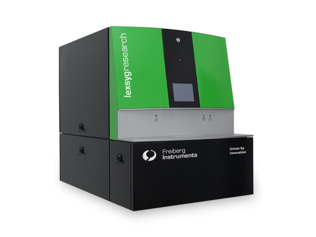
lexsygresearch

Skip breadcrumb navigation Breadcrumb Freiberg Instruments Products Luminescence Dating and Dosimetry lexsygresearch lexsyg research The most advanced TL/OSL reader Interested? Get in touch! Contact now Product Sheet Skip menu Quick navigation Features Applications Options Contact Features & Benefits Modular design: Interchangeable OSL stimulation units (up to 3 wavelengths per OSL), accommodates up to 4 detection units and up to 3 irradiation sources No crosstalk: Independent operation of measurement chamber and sample reservoir ensures absence of both stimulation and radiation crosstalk Nonstop operation: Ability to load and unload samples while another sample is undergoing analysis/treatment inside the measurement chamber Flexibility: Software controlled switch of detection filters within a measurement sequence Homogeneity: Highly homogeneous and stabilized optical stimulation provides identical measurement conditions Accessibility: IP based system allows remote operation and technical support from anywhere in the world Easy upgrade: Modular design allows future expansion of device capabilities by easily adding components Reference list – TL/OSL reader Applications Thermoluminescence (TL) Thermoluminescence (TL) is a backbone in radiation protection dosimetry with a long tradition and used for a wide range of dosimetric purposes, including accident dosimetry, retrospective… Learn more Photo/ Optically Stimulated Luminescence (PSL + OSL) Photostimulated Luminescence (PSL or POSL) is also called Optically Simulated Luminescence (OSL) and can be used for a wide range of dosimetric purposes. It is gaining importance in radiation… Learn more Radioluminescence Luminescence emitted during exposure to ionizing radiation can be employed for online dosimetry, e.g. in brachytherapy.Al2O3:C or BeO attached to optical fibres for online dosimetry can serve… Learn more Neutron dosimetry Active dosimeters, like rem-mteters, superheated emulsions and electronic personal dosemeters can be used to measure neutron fields. But frequently passive dosemeters are used to determine… Learn more Food Irradiation Control Food stuff often is irradiated with ionizing radiation for sterilisation purposes. This requires the detection and estimates of the applied doses. The attached mineral dust or the food itself… Learn more Medical dosimetry Ionizing radiation from a large variety of isotopic sources, as well as accelerators, electron beams, etc. are increasingly used in radiotherapy. Clinical diagnostics employing ionizing radiation… Learn more Luminescence spectroscopy Luminescence spectroscopy is used to investigate the luminescence properties of materials and thus allow more precise definitions e.g. of measurement parameters (e.g. detection ranges). It can… Learn more Spatially resolved luminescence Measuring luminescence with EMCCD camera allows for the spatial differentiation of luminescence signals. Different minerals, mineral phases, radiation hot spots etc. can be determined in granular… Learn more Time resolved luminescence Time resolved luminescence measurements allow the determination of the life-times of electron states and thus description of the kinetics involved. This allows the correlation to different… Learn more Optically stimulated Luminescence dating of quartz (OSL) Age range, Few years (depending on signal intensity and sensitivity of equipment for which the lexsyg systems are especially developed), Up to ~150-200,000 years (depending on dosimetry),… Learn more Infrared stimulated Luminescence dating of feldspar (IRSL) Due to higher saturation doses the age range is larger than for OSL, Internal dose rates in K-feldspar reduce dependency on external dose rate and water content, Might suffer from an anomalous… Learn more Single grain/spatially resolved luminescence dating Not every grain in a sediment sample reflects the same last bleaching and burial history. By analysing single mineral entities (whether grains or parts of it) different dose populations can be… Learn more Radiofluorescence Infrared-Radiofluorescence (IR-RF) is a technique for dosimetric dating of potassium feldspar to establish sedimentation ages. This method avoids some of the problems of other trapped-charge… Learn more Pulsing: mixed mineral samples Sometimes mineral separation in sediment or solid samples is not possible (polymineral samples), especially in cases of intergrowth of minerals. Pulsing (i.e. short light stimulation) the… Learn more Flint and other heated rocks Rocks containing amorphous/microcrystalline SiO2 can be dated by luminescence methods when they have been heated to approximately 400°C. Such temperatures, whether accidentally or deliberately,… Learn more Ceramics, pottery, bricks and statues While the typology of ceramics is a backbone of many archaeological chronologies, establishing the age directly for certain types of ceramics is sometimes required. Optically Stimulated… Learn more Unheated rock surfaces Granite or other quartz/feldspar containing rocks are preferentially dated with spatially resolved luminescence, Marble, limestone surfaces are dated with Optically Stimulated Luminescence (OSL)… Learn more Sediment dating Optically Stimulated Luminescence (OSL, TT-OSL) dating of quartz grains from sediments, Infrared Stimulated Luminescence (IRSL, pIRIR, IR-RF) dating of feldspar grains from sediments, Trench… Learn more Interested? Our experts are happy to assist you. Get in touch! Contact us now! Accessories & Options Configuration Options Automatic detector changer Irradiation sources Thermal stimulation Peltier cooling Pulsed OSL (10 µs) Red stimulated quartz OSL Filter wheel PMT detection unit InfraRedPhotoLuminescence (IRPL) X-ray Fluorescence (XRF) EMCCD Sample camera Spectrometry detection unit Bleaching/Solar simulation unit Ultra-fast pulsing (< 10 ns) Optional accessories Sample cups/discs Aliquot preparation kit LED head lamp Vacuum pump Air compressor Get in touch Do not hesitate to contact us – we are available to assist you with any inquiries or requests. Use our inquiry tool or reach out via email: sales @ freiberginstruments.com
Product

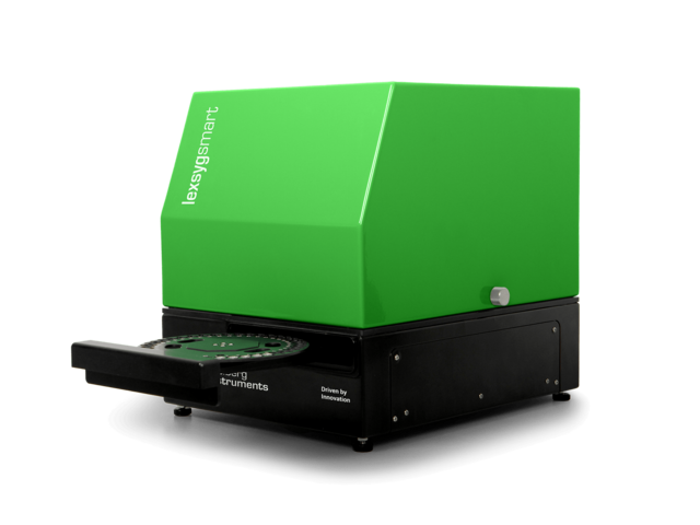
lexsygsmart

Skip breadcrumb navigation Breadcrumb Freiberg Instruments Products Luminescence Dating and Dosimetry lexsygsmart lexsyg smart The most sensitive TL/OSL reader Interested? Get in touch! Contact now Product Sheet Skip menu Quick navigation Features Applications Options Software Contact Features & Benefits Compact design: provides thermal and optical stimulation for up to 3 different wavelengths No crosstalk: independent operation of measurement chamber and sample changer ensures absence of stimulation and radiation crosstalk Flexibility: Software controlled switch of detection filters within a measurement sequence Homogeneity : highly homogeneous and stabilized optical stimulation provides identical measurement conditions Accessibility: IP based system allows remote operation and technical support from anywhere in the world Reference list – TL/OSL reader Applications Thermoluminescence (TL) Thermoluminescence (TL) is a backbone in radiation protection dosimetry with a long tradition and used for a wide range of dosimetric purposes, including accident dosimetry, retrospective… Learn more Photo/ Optically Stimulated Luminescence (PSL + OSL) Photostimulated Luminescence (PSL or POSL) is also called Optically Simulated Luminescence (OSL) and can be used for a wide range of dosimetric purposes. It is gaining importance in radiation… Learn more Neutron dosimetry Active dosimeters, like rem-mteters, superheated emulsions and electronic personal dosemeters can be used to measure neutron fields. But frequently passive dosemeters are used to determine… Learn more Food Irradiation Control Food stuff often is irradiated with ionizing radiation for sterilisation purposes. This requires the detection and estimates of the applied doses. The attached mineral dust or the food itself… Learn more Medical dosimetry Ionizing radiation from a large variety of isotopic sources, as well as accelerators, electron beams, etc. are increasingly used in radiotherapy. Clinical diagnostics employing ionizing radiation… Learn more Optically stimulated Luminescence dating of quartz (OSL) Age range, Few years (depending on signal intensity and sensitivity of equipment for which the lexsyg systems are especially developed), Up to ~150-200,000 years (depending on dosimetry),… Learn more Infrared stimulated Luminescence dating of feldspar (IRSL) Due to higher saturation doses the age range is larger than for OSL, Internal dose rates in K-feldspar reduce dependency on external dose rate and water content, Might suffer from an anomalous… Learn more Pulsing: mixed mineral samples Sometimes mineral separation in sediment or solid samples is not possible (polymineral samples), especially in cases of intergrowth of minerals. Pulsing (i.e. short light stimulation) the… Learn more Flint and other heated rocks Rocks containing amorphous/microcrystalline SiO2 can be dated by luminescence methods when they have been heated to approximately 400°C. Such temperatures, whether accidentally or deliberately,… Learn more Ceramics, pottery, bricks and statues While the typology of ceramics is a backbone of many archaeological chronologies, establishing the age directly for certain types of ceramics is sometimes required. Optically Stimulated… Learn more Unheated rock surfaces Granite or other quartz/feldspar containing rocks are preferentially dated with spatially resolved luminescence, Marble, limestone surfaces are dated with Optically Stimulated Luminescence (OSL)… Learn more Sediment dating Optically Stimulated Luminescence (OSL, TT-OSL) dating of quartz grains from sediments, Infrared Stimulated Luminescence (IRSL, pIRIR, IR-RF) dating of feldspar grains from sediments, Trench… Learn more Interested? Our experts are happy to assist you. Get in touch! Contact us now! Accessories & Options Configuration options Irradiation sources Thermal stimulation (TL) Pulsed OSL (10 µs) Red stimulated quartz OSL Filter wheel PMT detection unit Optional accessories Additional sample carousel Sample cups/discs Aliquot preparation kit LED head lamp Air compressor Software LexStudio 2.0 - Operating software Modern, professionally designed user interfacensitivity: Based on user feedback a new graphical user interface which combines clear arrangement and usability is developed by Freiberg… Learn more LexEva - Evaluation software LexEva is a newly released evaluation software developed for analysis in luminescence research and dating. LexEva was adapted to the "Luminescence" package developed by the R. Luminescence… Learn more TLStudio - Operating & Evaluation software User account management system, Transperent workflow, Professionally designed user interface, Intelligent parameter selection, Live data visualization, Easy programming of individual and… Learn more Get in touch Do not hesitate to contact us – we are available to assist you with any inquiries or requests. Use our inquiry tool or reach out via email: sales @ freiberginstruments.com
Product

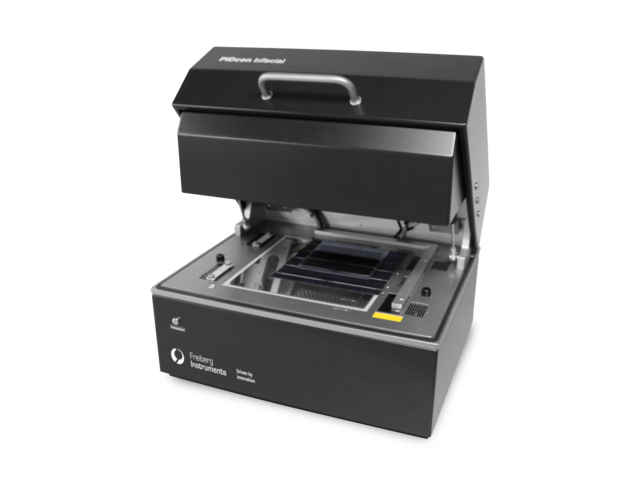
PIDcon bifacial

Skip breadcrumb navigation Breadcrumb Freiberg Instruments Products Potential Induced Degradation PIDcon bifacial PID con bifacial Quality Control Solution for Bifacial PERC/PERC+, HIT, Topcon, c-Si Solar Cells, Mini Modules, and More Interested? Get in touch! Contact now Product Sheet Skip menu Quick navigation Features Applications Specifications Technology Contact Benchtop PID tester for c-Si solar cells and mini-modules PID detection at cell level Research, Production & Quality Control of PERC, AL-BSF, PERC+, bifacial PERC, PERT, PERL and IBC solar cells No climate chamber necessary Features & Benefits Measurements of cells Test duration: 4 hours (typical) Voltage: ± 1.5 kV Module vs. Cell level PID test Applications Production Monitoring Potential Induced Degradation (PID) is a significant reliability issue in photovoltaic (PV) power plants. It is crucial to assess the susceptibility of products to PID early in the production… Learn more EVA Evaluation The PIDcon allows for the investigation of how EVA foil affects PID susceptibility using a sample stack that simulates a module. To perform the test, the user simply places a solar cell, the EVA… Learn more Solar Cell Classification Potential Induced Degradation (PID) poses a significant reliability issue in PV power plants, making it essential to assess products for their susceptibility to PID. The PIDcon system enables… Learn more Mini-module Classification Potential Induced Degradation (PID) is a critical reliability issue in PV power plants, making it essential to assess products for their susceptibility to PID. The PIDcon system helps… Learn more Glass Evaluation For more information please read:[1] V. Naumann, Ursachenanalyse und physikalische Modellbildung für potenzial-induzierte Degradation von Silizium-Solarzellen, Dissertation,… Learn more With our PIDcon bifacial testing device, module manufacturers can perform reliable quick tests of solar cells and encapsulation materials during production. Dr. Christian Hagendorf Key Account Manager Interested? Our experts are happy to assist you. Get in touch! Contact us now! Specifications Type Stress Recovery PID-s front 85 °C, +1.5 kV 85 °C, -1.5 kV PID-p rear 85 °C, +1.5 kV, without illumination 85 °C, dark storage or illumination PID-c rear 85 °C, +1.5 kV, with illumination Not possible Lamination 150 °C, 20 min Sample size up to 210 x 210 mm Suitable for For PERC, AL-BSF, IBC, PERC+, bifacial PERC p- and n-type Measurement of Measurement of: R parallel , leakage current, IV curve under illumination Download Product Sheet PDF (640 KB) Technologies Physical Nature of PID-s In the field a large potential between the front glass surface and the solar cells in a module can occur and a shunting of the p-n junction of a Si solar cell and accordingly a decrease in… Learn more Comparison of PID Test Methods The PIDcon test has the following advantages compared to other methods:Short duration (usually 4–8h), High variability: test of solar cell, mini-module, glass and EVA, Good control of test… Learn more Dependencies of PID Susceptibility For more information please read:[1] V. Naumann, Ursachenanalyse und physikalische Modellbildung für potenzial-induzierte Degradation von Silizium-Solarzellen, Dissertation,… Learn more Conductance Test and Power Loss Furthermore an easy pass or fail criterion after finishing the PID measurement is suggested. It is assumed that an efficiency loss of 3% at the end of the PID test lead to a fail of the solar… Learn more Get in touch Do not hesitate to contact us – we are available to assist you with any inquiries or requests. Use our inquiry tool or reach out via email: sales @ freiberginstruments.com
Product

Wafer XRD

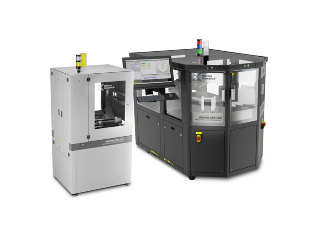
Skip breadcrumb navigation Breadcrumb Freiberg Instruments Products X-ray Diffraction Wafer XRD Wafer XRD / 200, 300 for fully automated sorting, sample crystalline orientation, sample dimension, optical notch/flat and edge profile determination and more Exclusively through Malvern Panalytical Contact for demo Product Sheet Skip menu Quick navigation Features Applications Technology Software Contact Materials With Wafer XRD, a wide variety of materials can be precisely analyzed. Thanks to their flexibility and performance, our systems meet even the most demanding requirements. Si SiC Quartz GaN GaAs AIN InP Al₂O₃ (sapphire) and more Features & Benefits Fully automated wafer handling and sorting system (eg: cassette to cassette) Crystal orientation and resistivity measurements Optical determination of geometric features (notch position, notch deep, notch opening angle, diameter, flat position and flat length) of wafers Distance measurement for unpolished wafers and mirroring surfaces MES and/or SECS/GEM interfaces Download Full characterization of semiconductor (SC) materials using the Wafer XRD200 (SC) tool PDF (289 KB) Fully automated wafer sorting and handling system Applications Automatic Wafer Sorting To ensure the exceptional performance required for semiconductors, every wafer must undergo thorough testing. The Omega-Scan method, known for its speed and precision, is ideal for fully… Learn more Wafer XRD – Exclusively through Malvern Panalytical This product is distributed by our trusted partner. Contact for demo Technologies Omega-scan Ultra-Fast Orientation Measurement for Single Crystals Learn more Theta-scan Precision X-ray Method for Single Crystal Orientation Learn more Software XRDStudio Multiple Operating ModesOperator Mode: Designed for fixed measurement parameters, ensuring a safe and streamlined workflow. Administrator Mode: Allows for the creation and modification of… Learn more Wafer XRD – Exclusively through Malvern Panalytical This product is distributed by our trusted partner. Contact for demo

Product

Quartz XRD

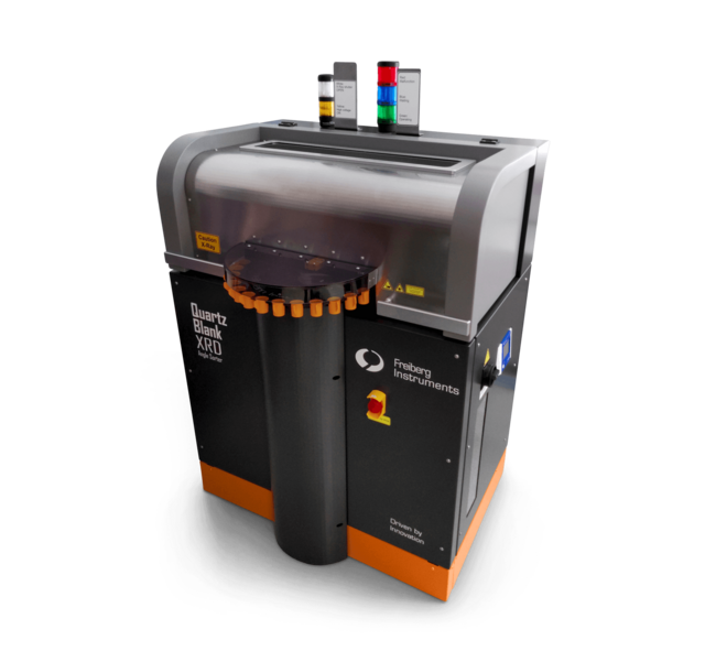
Skip breadcrumb navigation Breadcrumb Freiberg Instruments Products X-ray Diffraction Quartz XRD Quartz XRD Bars, Wafers and Blanks using X-ray Diffractometer (XRD) Interested? Get in touch! Contact now Product Sheet Skip menu Quick navigation Features Software Contact Features & Benefits Measurement speed: as low as 2 s (AT quartz) Highest precision: ≤ 10 arcsec standard deviation Spatial resolution: 1 mm ± 0.1 mm Determination of orientation inclination relative to the sample Automatic display of angular components (Theta & Phi) including standard deviation German engineering: robust and modular design Software: easy-to-use software suite with multiple user levels. Automatic display, recording and reporting of measurement data Automation: Customized sample handling systems for different size wafers or blanks, including robot, pick & place, vibratory feeder XRD series Quartz Blank XRD Learn more XRD series Quartz Wafer XRD Learn more XRD series Quartz Bar XRD Learn more Details MES interface for Industry Mapping (wafers) Stereographical projection and more X-ray tube: 1.5 kW, Cu anode Power supply: 100 - 230 V, 16 A, single phase Download Product Sheet PDF (1 MB) Last revision: 14th June, 2022 Interested? Our experts are happy to assist you. Get in touch! Contact us now! Software XRDStudio Multiple Operating ModesOperator Mode: Designed for fixed measurement parameters, ensuring a safe and streamlined workflow. Administrator Mode: Allows for the creation and modification of… Learn more Get in touch Do not hesitate to contact us – we are available to assist you with any inquiries or requests. Use our inquiry tool or reach out via email: sales @ freiberginstruments.com
Product

Quartz Wafer XRD

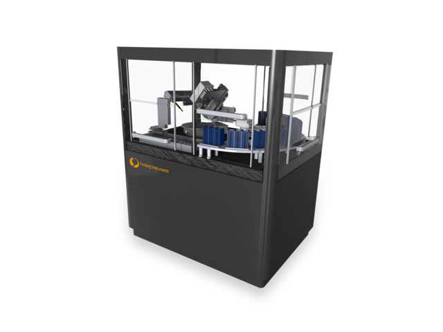
Skip breadcrumb navigation Breadcrumb Freiberg Instruments Products X-ray Diffraction Quartz XRD Quartz Wafer XRD Quartz Wafer XRD Enable tight frequency specs in mass production Interested? Get in touch! Contact now Product Sheet Skip menu Quick navigation Features Applications Technology Contact Quartz Wafer orientation and sorting in a modular package Modular Design Sample size from 4mm x 4mm to 80mm x 80mm 350 wafers/h throughput at standard sorting accuracy Materials The Quartz Wafer XRD enables high-throughput and high-precision in a modular design that can split CapEx in stages. Quartz and more Features & Benefits CapEx Friend Modular Design 350 wafers/h At standard sorting accuracy 4mm - 80mm Wafer dimension 40 Years Quartz Experience 40 Years Quartz Experience Fully automated quartz wafer analysing machine Samples: Round, rectangular & square 4 x 4 mm up to 80 x 80 mm (manual sample handling) 20 x 20 mm up to 80 x 80 mm (automatic sample handling) Features: Mapping option for spatial quality check Modular design allows future automation upgrade Standard sample holders for input/output: cassettes or stacks Sorting function available Throughput: up to 350 wafers/h at standard sorting accuracy Applications Automatic Wafer Sorting To ensure the exceptional performance required for semiconductors, every wafer must undergo thorough testing. The Omega-Scan method, known for its speed and precision, is ideal for fully… Learn more Interested? Our experts are happy to assist you. Get in touch! Contact us now! Technologies Omega-scan Ultra-Fast Orientation Measurement for Single Crystals Learn more Theta-scan Precision X-ray Method for Single Crystal Orientation Learn more Get in touch Do not hesitate to contact us – we are available to assist you with any inquiries or requests. Use our inquiry tool or reach out via email: sales @ freiberginstruments.com
Product

Quartz Blank XRD

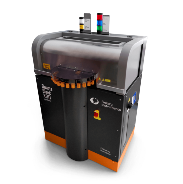
Skip breadcrumb navigation Breadcrumb Freiberg Instruments Products X-ray Diffraction Quartz XRD Quartz Blank XRD Quartz Blank XRD Enable tight frequency specs in mass production Interested? Get in touch! Contact now Product Sheet Skip menu Quick navigation Features Applications Technology Contact Quartz blank orientation and sorting at warp speed Automated sorting options for round, rectangular and square samples Orientation binning down to ±7.5 arcsec 1000 blanks/h throughput at standard sorting accuracy Materials The Quartz Blank XRD enables high-throughput and high-precision orientation binning of quartz blanks and more Quartz Features & Benefits ± 7.5 arcsec Minimum sorting group size 1000 blanks/ At standard sorting accuracy 1.5mm - 12mm Blank dimension 40 years Quartz Experience 40 years Quartz Experience Samples: Round, rectangular & square 4 x 4 mm up to 12 x 12 mm (manual sample handling) 1.5 x 1.5 mm up to 3.0 x 6.0 mm (automation option I) 4.0 x 4.0 mm up to 9.0 x 9.0 mm (automation option II) Features: Sorting into quality groups: ± 7.5 arcsec (minimum) Throughput: up to 1000 blanks/h at standard sorting accuracy Applications Quartz Blank Sorting Quartz blanks are the core component of oscillator devices, each resonating at a specific frequency. The stability of this frequency under varying temperatures is determined by the quartz's… Learn more Interested? Our experts are happy to assist you. Get in touch! Contact us now! Technologies Omega-scan Ultra-Fast Orientation Measurement for Single Crystals Learn more Theta-scan Precision X-ray Method for Single Crystal Orientation Learn more Get in touch Do not hesitate to contact us – we are available to assist you with any inquiries or requests. Use our inquiry tool or reach out via email: sales @ freiberginstruments.com
Product

Quartz Bar XRD

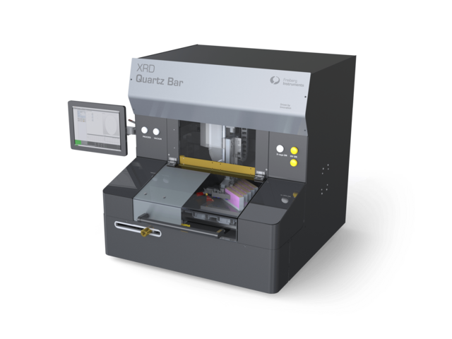
Skip breadcrumb navigation Breadcrumb Freiberg Instruments Products X-ray Diffraction Quartz XRD Quartz Bar XRD Quartz Bar XRD Enable tight frequency specs in mass production Interested? Get in touch! Contact now Product Sheet Skip menu Quick navigation Features Applications Technology Contact Automate your Quartz bar orientation and glueing process. Workflow aligned automation Integrated glueing and orientation measurement 40 years of Quartz orientation experience Materials The Quartz Bar XRD enables high-throughput and high-precision sawing preparation and more Quartz Features & Benefits ±0.5°(AT&TF) Alignment precision Automated gluing On Adapter Plate Bar Uptake Fully automated 10s Measurement speed for high throughput 10s Measurement speed for high throughput Fully automated quartz bar aligning machine Samples: quartz bars Handling: Fully automated uptake and alignment of quartz bars Automated gluing on adapter plate Alignment precision: ± 0.5° (AT & TF) Applications Quartz Bar Aligning Quartz bars serve as the raw material for cutting high-quality blanks with precise temperature characteristics. Proper pre-alignment is essential to ensure optimal performance. To achieve… Learn more Interested? Our experts are happy to assist you. Get in touch! Contact us now! Technologies Omega-scan Ultra-Fast Orientation Measurement for Single Crystals Learn more Theta-scan Precision X-ray Method for Single Crystal Orientation Learn more Get in touch Do not hesitate to contact us – we are available to assist you with any inquiries or requests. Use our inquiry tool or reach out via email: sales @ freiberginstruments.com
Product

Angle Sorter

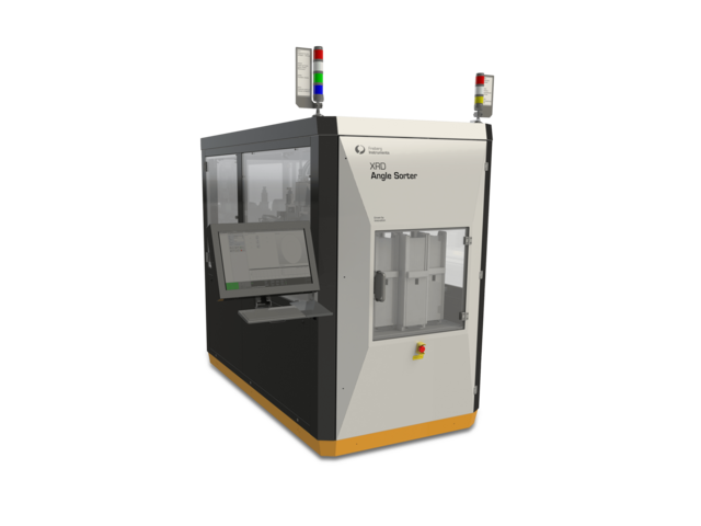
Skip breadcrumb navigation Breadcrumb Freiberg Instruments Products X-ray Diffraction Angle Sorter Angle Sorter This product launching soon Interested? Get in touch! Contact now Skip menu Quick navigation Applications Technology Contact Applications Automatic Wafer Sorting To ensure the exceptional performance required for semiconductors, every wafer must undergo thorough testing. The Omega-Scan method, known for its speed and precision, is ideal for fully… Learn more Interested? Our experts are happy to assist you. Get in touch! Contact us now! Technologies Omega-scan Ultra-Fast Orientation Measurement for Single Crystals Learn more Theta-scan Precision X-ray Method for Single Crystal Orientation Learn more Get in touch Do not hesitate to contact us – we are available to assist you with any inquiries or requests. Use our inquiry tool or reach out via email: sales @ freiberginstruments.com
Product

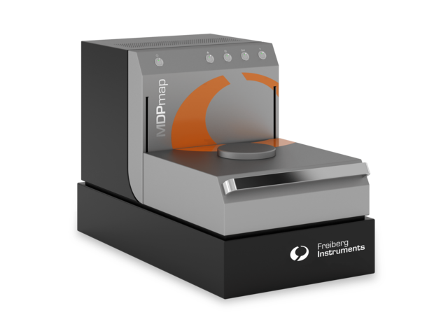
MDPmap

Skip breadcrumb navigation Breadcrumb Freiberg Instruments Products Microwave Detected Photoconductivity MDPmap MDPmap Precision Lifetime Charachterization with Exceptional Sensitivity Interested? Get in touch! Contact now Product Sheet Laser Selection Guide Skip menu Quick navigation Features Applications Specifications Technology Options Contact Advanced R&D – destruction free, flexible and fast Highly sensitive due to advanced microwave system Customized laser and optic integration for all your materials Simultaneous resistivity measurement and other options Materials The MDPmap features a versatile selection of advanced lasers, enabling comprehensive electrical characterization for nearly all types of semiconductors. Si SiC Ge GaAs Ga₂O₃ InP Diamond and more Features & Benefits 355–1550 nm Available wavelengths 10 ns Time resolution > 99 % repeatability Resistivity 0.3–5 Ohm cm Resistivity 0.3–5 Ohm cm Sensitivity: highest sensitivity for visualization of so far invisible defects and investigations of epitaxial layers Measurement speed: < 5 minutes for a 6 inch Si wafer, 1 mm resolution Range of lifetimes: 20 ns to several ms Contamination determination : metal (Fe) contaminations originated in crucibles and equipment Measurement capability: from as-cut wafers to fully processed samples Flexibility: fixed measurement head allows coupling of external lasers with trigger Reliability: modular and compact bench top instrument for higher reliability and uptime > 99% Repeatability: > 99% Resistivity: resistivity mapping without frequent calibration MDPmap - Mono-and Multi-crystalline wafer lifetime measurement device (µPCD/MDP(QSS)) Flexible mapping tool for R&D or production monitoring MDPmap is designed as a compact bench top contactless electrical characterization tool for offline production control or R&D, measuring parameters like carrier lifetime, photoconductivity, resistivity and defect information over a wide injection range in steady state or short pulse excitation (μ-PCD). Automated sample recognition and parameter setup allows an easy adaption to a big variety of different samples comprising epitaxial layers and wafers after various preparation stages ranging from as-grown wafers to up to 95% metallized ones. The major advantage of MDPmap is its high flexibility, which allows for instance the integration of up to four lasers either for injection level dependent lifetime measurements ranging from ultra low to high injection or extracting depth information by using different laser wavelengths. Bias light facility is included as well as options for μ-PCD or steady state injection conditions. A customer defined calculation with different maps is possible as well as an export of primary data for further evaluation. For standard metrology tasks a predefined standard enables routine measurements by only pushing one button. Lifetime map of passivated multicrystalline silicon Iron contamination map of multicrystalline silicon Bor oxygen map of mono silicon Trap density map of mono silicon Applications Photoconductivity measurements and trap analysis Equipped with a 355 nm laser (μ-PCD) or a 375 nm laser diode (MDP), the MDPmap as well as the MDpicts from Freiberg Instruments are suitable for photoconductivity measurements and trap analysis… Learn more Resistance measurements on wafers and bricks With MDPmap and MDPingot it is possible to measure the resistivity of wafers or bricks with a high accuracy and a resolution of 1 mm via eddy current measurements. The Eddy current sensor setup… Learn more Light Beam Induced Current (LBIC) The proceeding is based on the measurement of the local short circuit current Isc in the cell, which is produced through appropriate excitation. For the measurement the solar cell is contacted… Learn more Minority carrier Lifetime maps on 450 mm wafers Since several years, the microelectronic industry is planning to enlarge the wafer size from 300 mm (12 inch) to 450 mm (18 inch) diameter, in order to gain more yield. The technology for the… Learn more Iron concentration determination With the MDPingot and MDPmap series it is possible to measure the iron concentration in bricks and wafers fully automated and with a very high resolution. Lifetime measurements before and after… Learn more Minority carrier lifetime measurements on SiC In recent years the quality of SiC materials has improved profoundly and hence SiC is becoming more and more a competitor to Si for e.g. high-power devices. Since it is a wide-bandgap… Learn more Investigation of material quality of GaAs In contrast to other techniques MD-PICTS (microwave detected photo induced current transient spectroscopy) can detect signals even from thin surface regions (3 µm) of SI GaAs samples and is… Learn more Detection of CrB in silicon Lifetime measurements before and after chromium boron pair dissociation is a widely used method for chromium determination in silicon wafers. In boron doped silicon with a high doping… Learn more Detection of BO2 in silicon The boron-oxygen complexes can be activated by irradiating the sample with light and deactivated by heating the sample at 200 °C for several minutes. This can be used similar to the iron… Learn more Trap concentration determination With the MDPmap and MDPingot it is possible to measure the photoconductivity as well as the minority carrier lifetime with one measurement and fully automated in a wide injection range. A clever… Learn more Injection dependent measurements With MDPmap it is possible to measure not only injection dependent lifetime curves but also photoconductivity curves over a very wide range of injection. In the MDPmap and MDPingot up to 4… Learn more Highly spatial resolved inline metrology on Multicrystalline Silicon Non-destructive measurements of minority carrier lifetime are well established and widely used for process control and characterization of defects in crystalline silicon. With our tool MDPinline… Learn more Determination of passivation homogeneity and surface recombination vel The measured or effective lifetime consists of the bulk lifetime and the surface lifetime, via: \(\cfrac{1}{\tau_{eff}} = \cfrac{1}{\tau_{bulk}} + \cfrac{1}{\tau_{surface}}\) That‘s why the… Learn more Photoconductivity measurements of implanted samples In this case not the lifetime, but the photoconductivity or signal height is the most sensitive parameter for detecting inhomogeneity in implantations. It depends strongly on the resistivity and… Learn more Lifetime determination of epitaxial silicon thin-film layers With MDP it is possible to measure the lifetime of minority carriers and the photoconductivity in epitaxial layers as fast and exactly as possible with a high resolution. The measurement of… Learn more Interested? Our experts are happy to assist you. Get in touch! Contact us now! Technical specifications sample size up to 300 mm diameter (standard), up to 450 mm diameter (on request), down to 5 x 5 mm range of lifetimes 20 ns to several ms resistivity 0.2 - >10 3 Ohm cm, p/n material silicon wafer, epi layers, partially or fully processed wafers, compound semiconductors and beyond measureable properties lifetime - μ-PCD/MDP (QSS), photoconductivity excitation select up to four different wavelengths from 355 nm up to 1480 nm. 980 nm (default) dimensions 680 x 380 x 450 mm, weight: ca. 65 kg power 100 - 250V, 50/60 Hz, 5 A Technologies Minority carrier lifetime The measured effective lifetime is composed of the bulk lifetime and surface lifetime, which depends on the surface properties of a sample. Hence the surface has to be passivated, if you want… Learn more Photoconductivity When light of sufficient energy is absorbed by a semiconductor, the number of free electrons and holes changes and raises the electrical conductivity of the semiconductor. This increase is… Learn more Resistivity The electrical resistivity directly depends on the density of the semiconductor and is therefore a useful parameter to monitor doping profiles and homogeneity. The lifetime and diffusion length… Learn more Mobility The mobility is a quantity related to the drift velocity of electrons or holes in an applied electric field across a material. The mobility depends on different scattering processes that can… Learn more Diffusion length Learn more Defect properties The properties of a defect and its impact on the material quality can be described by three main parameters:defect concentration NT, capture cross sections for electrons and holes σn, σp,… Learn more Lifetime simulations From the simulated time dependent carrier concentrations the photoconductivity can be calculated using the mobility model of DORKEL and LETURCQ [2] . The minority carrier lifetime can be… Learn more Simulation of carrier profiles The measurement of thick samples as bricks leads to new questions and problems. One of these questions is how the carrier profiles that develops in a sample effect the lifetime measurements. To… Learn more Microwave detected photoconductivity (MDP) The novel method MDP is well suited for both, defect investigation by e.g. injection dependent minority carrier lifetime measurements, as well as mapping of wafers or even bricks for inline… Learn more Comparison to µ-PCD and QSSPC Besides MDP the two most important contact less lifetime measuring methods are QSSPC (quasi steady state photoconductivity) and µ-PCD (microwave detected photoconductive decay). Currently one… Learn more MD-PICTS MD-PICTS is a modification of MDP, where temperature dependent measurements of the defect part of the transient are accomplished. This allows for a spatially resolved defect characterization.… Learn more Penetration depth of different laser wavelength in silicon The microwave detected photoconductivity measures the photoconductivity after the irradiation of the sample with light. Usually the light should have an energy that is higher than the bandgap,… Learn more Materials Electrical properties and defects of a large variety of semiconductor materials, devices and dielectric materials can be investigated contact less and destruction with our advanced method MDP.… Learn more Accessories & Options Our devices offer versatile configuration options to meet specific requirements effectively. Each model can be customized to ensure maximum flexibility and efficiency. Contact for more information Spot size variation Resistivity measurement (wafers) Sheet resistance Background/Bias light Reflection measurement (MDP) LBIC for solar cells Reference wafer Internal/External iron mapping of Si Integrated heating stage Wide range of lasers Get in touch Do not hesitate to contact us – we are available to assist you with any inquiries or requests. Use our inquiry tool or reach out via email: sales @ freiberginstruments.com