Found 271 results in 2 milliseconds.

Application

Solar Cell Classification

Solar Cell Classification The PIDcon enables quick, routine quality control of solar cell PID susceptibility, unaffected by the EVA foil and glass Potential Induced Degradation (PID) poses a significant reliability issue in PV power plants, making it essential to assess products for their susceptibility to PID. The PIDcon system enables manufacturers to test their products as early as possible in the production process, starting at the solar cell level, and to evaluate the encapsulation materials as well. This allows for independent investigation of the solar cell and its SiNx layer, separate from the effects of the EVA and glass. The type of PID considered here involves shunting of solar cells due to high-voltage stress-induced leakage currents (PID-s). To effectively classify solar cells, it is crucial to use sensitive EVA and glass materials so that the solar cell itself becomes the critical factor influencing the PID susceptibility of the entire stack. A lamination step can be added prior to measurement to enhance comparability with actual modules. The solar cells are connected using gold contact pins, which can be adjusted to fit the busbar design, even for island busbars. The PIDStudio software allows users to set pass/fail criteria for the test, suggesting defaults based on IEC standards and insights from Fraunhofer CSP scientists. Fig. 1: Solar cell with EVA foil and glass placed in a PIDcon Matching Products PID series PIDcon bifacial Quality Control Solution for Bifacial PERC/PERC+, HIT, Topcon, c-Si Solar Cells, Mini Modules, and More Learn more Get in touch Do not hesitate to contact us – we are available to assist you with any inquiries or requests. Use our inquiry tool or reach out via email: sales @ freiberginstruments.com

Application

Mini-module Classification

Mini-module Classification The PIDcon benchtop system offers fast, cost-effective routine quality control for mini-modules' PID susceptibility, without the need for a climate chamber Potential Induced Degradation (PID) is a critical reliability issue in PV power plants, making it essential to assess products for their susceptibility to PID. The PIDcon system helps manufacturers test products earlier in the production chain, such as mini-modules. The PID in question refers to the shunting of solar cells caused by high-voltage stress-induced leakage currents (PID-s). Mini-modules are contacted at two points, with a contact check ensuring proper connection. The PIDStudi o software allows users to define pass/fail criteria and also provides recommended settings based on IEC standards and the expertise of Fraunhofer CSP scientists. Matching Products PID series PIDcon bifacial Quality Control Solution for Bifacial PERC/PERC+, HIT, Topcon, c-Si Solar Cells, Mini Modules, and More Learn more Get in touch Do not hesitate to contact us – we are available to assist you with any inquiries or requests. Use our inquiry tool or reach out via email: sales @ freiberginstruments.com

Application

Glass Evaluation

Glass Evaluation Glass resistivity is key to PID susceptibility and must be tested independently from the solar cell and EVA Since the PV community recognized the PID issue, extensive research has shown that both the solar cell and its SiNx layer, as well as the encapsulation materials, significantly impact a module's PID susceptibility. In addition to the polymer foil, the glass also plays a critical role and needs to be evaluated. The PIDcon system allows for the assessment of glass influence on PID susceptibility. Using a sample stack that simulates a module, the user simply places the solar cell, EVA foil, and the glass to be tested. For accurate comparison, solar cells from the same batch and the same EVA foil should be used. Table 1 presents the ion analysis of various glass types tested via ICP. Table 1: Ion analysis of the investigated glass types by ICP Fig. 1: PIDcon measurement with the same type of solar cell and EVA foil and different glass types Fig. 2: dependency of the decrease in parallel resistance on the glas type [1] For more information please read: [1] V. Naumann, Ursachenanalyse und physikalische Modellbildung für potenzial-induzierte Degradation von Silizium-Solarzellen, Dissertation, Martin-Luther-Universität Halle-Wittenberg (2014) Matching Products PID series PIDcon bifacial Quality Control Solution for Bifacial PERC/PERC+, HIT, Topcon, c-Si Solar Cells, Mini Modules, and More Learn more Get in touch Do not hesitate to contact us – we are available to assist you with any inquiries or requests. Use our inquiry tool or reach out via email: sales @ freiberginstruments.com

Product

Quartz Bar XRD

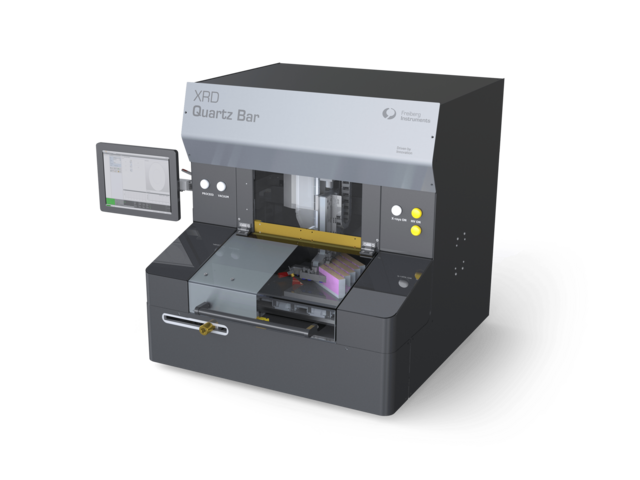
Skip breadcrumb navigation Breadcrumb Freiberg Instruments Products X-ray Diffraction Quartz XRD Quartz Bar XRD Quartz Bar XRD Enable tight frequency specs in mass production Interested? Get in touch! Contact now Product Sheet Skip menu Quick navigation Features Applications Technology Contact Automate your Quartz bar orientation and glueing process. Workflow aligned automation Integrated glueing and orientation measurement 40 years of Quartz orientation experience Materials The Quartz Bar XRD enables high-throughput and high-precision sawing preparation and more Quartz Features & Benefits ±0.5°(AT&TF) Alignment precision Automated gluing On Adapter Plate Bar Uptake Fully automated 10s Measurement speed for high throughput 10s Measurement speed for high throughput Fully automated quartz bar aligning machine Samples: quartz bars Handling: Fully automated uptake and alignment of quartz bars Automated gluing on adapter plate Alignment precision: ± 0.5° (AT & TF) Applications Quartz Bar Aligning Quartz bars serve as the raw material for cutting high-quality blanks with precise temperature characteristics. Proper pre-alignment is essential to ensure optimal performance. To achieve… Learn more Interested? Our experts are happy to assist you. Get in touch! Contact us now! Technologies Omega-scan Ultra-Fast Orientation Measurement for Single Crystals Learn more Theta-scan Precision X-ray Method for Single Crystal Orientation Learn more Get in touch Do not hesitate to contact us – we are available to assist you with any inquiries or requests. Use our inquiry tool or reach out via email: sales @ freiberginstruments.com

Product

Quartz Wafer XRD

Skip breadcrumb navigation Breadcrumb Freiberg Instruments Products X-ray Diffraction Quartz XRD Quartz Wafer XRD Quartz Wafer XRD Enable tight frequency specs in mass production Interested? Get in touch! Contact now Product Sheet Skip menu Quick navigation Features Applications Technology Contact Quartz Wafer orientation and sorting in a modular package Modular Design Sample size from 4mm x 4mm to 80mm x 80mm 350 wafers/h throughput at standard sorting accuracy Materials The Quartz Wafer XRD enables high-throughput and high-precision in a modular design that can split CapEx in stages. Quartz and more Features & Benefits CapEx Friend Modular Design 350 wafers/h At standard sorting accuracy 4mm - 80mm Wafer dimension 40 Years Quartz Experience 40 Years Quartz Experience Fully automated quartz wafer analysing machine Samples: Round, rectangular & square 4 x 4 mm up to 80 x 80 mm (manual sample handling) 20 x 20 mm up to 80 x 80 mm (automatic sample handling) Features: Mapping option for spatial quality check Modular design allows future automation upgrade Standard sample holders for input/output: cassettes or stacks Sorting function available Throughput: up to 350 wafers/h at standard sorting accuracy Applications Automatic Wafer Sorting To ensure the exceptional performance required for semiconductors, every wafer must undergo thorough testing. The Omega-Scan method, known for its speed and precision, is ideal for fully… Learn more Interested? Our experts are happy to assist you. Get in touch! Contact us now! Technologies Omega-scan Ultra-Fast Orientation Measurement for Single Crystals Learn more Theta-scan Precision X-ray Method for Single Crystal Orientation Learn more Get in touch Do not hesitate to contact us – we are available to assist you with any inquiries or requests. Use our inquiry tool or reach out via email: sales @ freiberginstruments.com

Product

Quartz Blank XRD

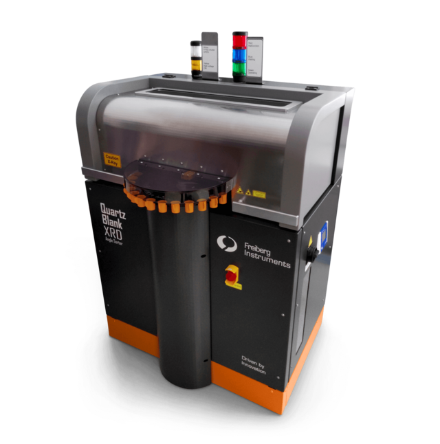
Skip breadcrumb navigation Breadcrumb Freiberg Instruments Products X-ray Diffraction Quartz XRD Quartz Blank XRD Quartz Blank XRD Enable tight frequency specs in mass production Interested? Get in touch! Contact now Product Sheet Skip menu Quick navigation Features Applications Technology Contact Quartz blank orientation and sorting at warp speed Automated sorting options for round, rectangular and square samples Orientation binning down to ±7.5 arcsec 1000 blanks/h throughput at standard sorting accuracy Materials The Quartz Blank XRD enables high-throughput and high-precision orientation binning of quartz blanks and more Quartz Features & Benefits ± 7.5 arcsec Minimum sorting group size 1000 blanks/ At standard sorting accuracy 1.5mm - 12mm Blank dimension 40 years Quartz Experience 40 years Quartz Experience Samples: Round, rectangular & square 4 x 4 mm up to 12 x 12 mm (manual sample handling) 1.5 x 1.5 mm up to 3.0 x 6.0 mm (automation option I) 4.0 x 4.0 mm up to 9.0 x 9.0 mm (automation option II) Features: Sorting into quality groups: ± 7.5 arcsec (minimum) Throughput: up to 1000 blanks/h at standard sorting accuracy Applications Quartz Blank Sorting Quartz blanks are the core component of oscillator devices, each resonating at a specific frequency. The stability of this frequency under varying temperatures is determined by the quartz's… Learn more Interested? Our experts are happy to assist you. Get in touch! Contact us now! Technologies Omega-scan Ultra-Fast Orientation Measurement for Single Crystals Learn more Theta-scan Precision X-ray Method for Single Crystal Orientation Learn more Get in touch Do not hesitate to contact us – we are available to assist you with any inquiries or requests. Use our inquiry tool or reach out via email: sales @ freiberginstruments.com

Product

XRDmap Pro

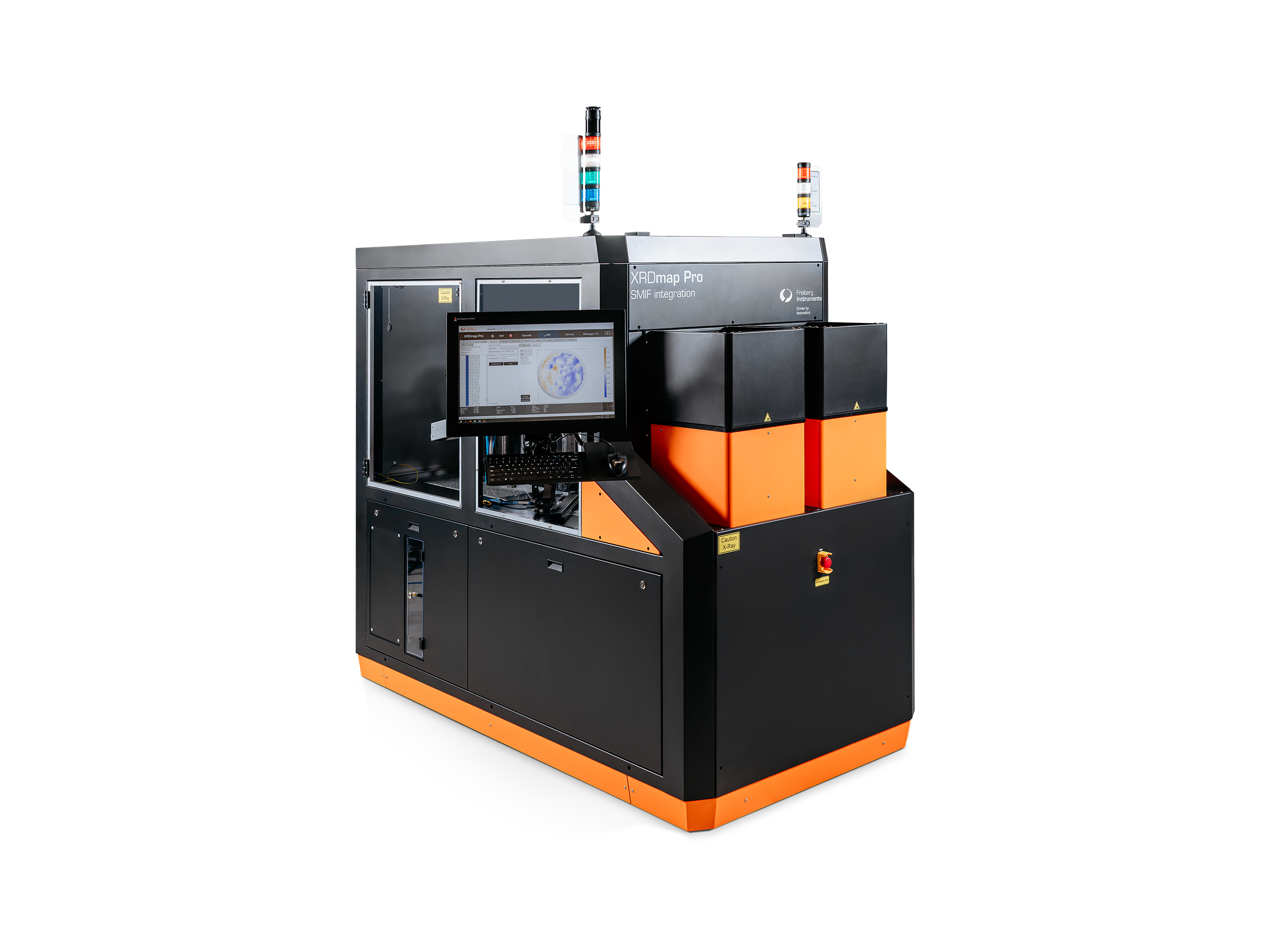
Skip breadcrumb navigation Breadcrumb Freiberg Instruments Products X-ray Diffraction XRDmap Pro XRDmap Pro Wafer Edition Inline wafer orientation mapping truly fab compliant Interested? Get in touch! Contact now Skip menu Quick navigation Features Applications Technology Software Contact Optimize wafer alignment inline for higher productivity. Ultra-fast hybrid X-ray optical metrology with proprietary algorithm Full automation featuring SMIF Loadports suitable for OHT connection Grows with your expansion: 70mm-230mm Wafersize flexibility Materials The XRDmap Pro Wafer Edition enables maximum value add by tuning subsequent processes such as epitaxy, lithography and implanting to the crystal orientation. This enables supplier process compliance and a smooth material flow by its ultra-fast measurement speed and seamless factory automation. Si Ge GaAs GaN Ga₂O₃ Diamond InP and more Features & Benefits 70–200mm Wafer Size 0.003˚ Offcut magnitude precision Flexible Loading and communication options Measured by opt. sensors Wafer Geometry Measured by opt. sensors Wafer Geometry Applications Crystal Surface Orientation Mapping Even within a single crystal, slight variations in crystal orientation can occur across the surface, often due to internal strains from lattice defects. Similarly, well-grown thin films can… Learn more Interested? Our experts are happy to assist you. Get in touch! Contact us now! Technologies Omega-scan Ultra-Fast Orientation Measurement for Single Crystals Learn more Software XRDStudio Multiple Operating ModesOperator Mode: Designed for fixed measurement parameters, ensuring a safe and streamlined workflow. Administrator Mode: Allows for the creation and modification of… Learn more Get in touch Do not hesitate to contact us – we are available to assist you with any inquiries or requests. Use our inquiry tool or reach out via email: sales @ freiberginstruments.com

Product

MDPpro

Skip breadcrumb navigation Breadcrumb Freiberg Instruments Products Microwave Detected Photoconductivity MDPpro MDPpro Advanced Lifetime Measurement System for Quality Control and Material R&D on Semiconductors Interested? Get in touch! Contact now Product Sheet Laser Selection Guide Skip menu Quick navigation Features Applications Options Contact Materials Sophisticated Material Research & DevelopmentFew examples for research applications, Iron concentration determination Trap concentration determination Boron oxygen determination Injection dependent measurements and more Si SiC compound semiconductor Ge GaAs CdTe InP ZnS Perovskite oxides wide bandgap materials epitaxial layers and more Features & Benefits Throughput >240 bricks/day Speed > 99% Repeatability 1 mm cutting criteria for 156x156x400 m brick quality monitoring quality monitoring Contactless and destruction free lifetime imaging (μPCD/MDP (QSS)), photoconductivity, resistivity and p/n check according to semi standard SEMI PV9-1110 Wafer cutting, Furnace monitoring, Material optimization and more Best throughput: >240 bricks/day or >720 wafers/day Measurement speed: <4 minutes for a 156 x 156 x 400 mm standard brick Yield improvement : 1 mm cutting criteria for a 156 x 156 x 400 mm standard brick Quality control: designed for quality monitoring of processes and materials like mono or multi-crystalline silicon Contamination determination: metal (Fe) contaminations originated in crucibles and equipment Reliability: modular and rugged industrial instrument for higher reliability and uptime > 99% Repeatability: > 99% Resistivity: resistivity mapping without frequent calibration Facts completely contactless destruction free electrical semiconductor characterisation special “underneath the surface” lifetime measurement technique advanced sensitivity for visualisation of so far invisible defects automated cut criteria definition spacial resolved p/n conduction type transformation detection Applications Resistance measurements on wafers and bricks With MDPmap and MDPingot it is possible to measure the resistivity of wafers or bricks with a high accuracy and a resolution of 1 mm via eddy current measurements. The Eddy current sensor setup… Learn more Light Beam Induced Current (LBIC) The proceeding is based on the measurement of the local short circuit current Isc in the cell, which is produced through appropriate excitation. For the measurement the solar cell is contacted… Learn more Minority carrier Lifetime maps on 450 mm wafers Since several years, the microelectronic industry is planning to enlarge the wafer size from 300 mm (12 inch) to 450 mm (18 inch) diameter, in order to gain more yield. The technology for the… Learn more Iron concentration determination With the MDPingot and MDPmap series it is possible to measure the iron concentration in bricks and wafers fully automated and with a very high resolution. Lifetime measurements before and after… Learn more p/n detection in bricks In the PV industry sometimes also low quality material with a high phosphorous concentration is used. Phosphor has a segregation coefficient of 0.35 and is therefore segregating in the top of the… Learn more Detection of CrB in silicon Lifetime measurements before and after chromium boron pair dissociation is a widely used method for chromium determination in silicon wafers. In boron doped silicon with a high doping… Learn more Detection of BO2 in silicon The boron-oxygen complexes can be activated by irradiating the sample with light and deactivated by heating the sample at 200 °C for several minutes. This can be used similar to the iron… Learn more Trap concentration determination With the MDPmap and MDPingot it is possible to measure the photoconductivity as well as the minority carrier lifetime with one measurement and fully automated in a wide injection range. A clever… Learn more Injection dependent measurements With MDPmap it is possible to measure not only injection dependent lifetime curves but also photoconductivity curves over a very wide range of injection. In the MDPmap and MDPingot up to 4… Learn more Inline metrology of mc-Si bricks With the MDPinline ingot it is possible to measure all 4 sides of a brick in under 1 min per side with 1 mm resolution. At the same time a spatial resolved measurement of conduction type changes… Learn more Highly spatial resolved inline metrology on Multicrystalline Silicon Non-destructive measurements of minority carrier lifetime are well established and widely used for process control and characterization of defects in crystalline silicon. With our tool MDPinline… Learn more Determination of passivation homogeneity and surface recombination vel The measured or effective lifetime consists of the bulk lifetime and the surface lifetime, via: \(\cfrac{1}{\tau_{eff}} = \cfrac{1}{\tau_{bulk}} + \cfrac{1}{\tau_{surface}}\) That‘s why the… Learn more Photoconductivity measurements of implanted samples In this case not the lifetime, but the photoconductivity or signal height is the most sensitive parameter for detecting inhomogeneity in implantations. It depends strongly on the resistivity and… Learn more Lifetime determination of epitaxial silicon thin-film layers With MDP it is possible to measure the lifetime of minority carriers and the photoconductivity in epitaxial layers as fast and exactly as possible with a high resolution. The measurement of… Learn more Interested? Our experts are happy to assist you. Get in touch! Contact us now! Accessories & Options Spot size variation Resistivity measurement (bricks/wafers) Background/Bias light Reflection measurement (MDP) LBIC BiasMDP LBIC for solar cells LBIC, BiasMDP measurement stage with contacts Reference wafer Resistivity calibration set (bricks/wafers) Internal iron mapping of Si P/N detection Bar code reader Wide range of lasers Get in touch Do not hesitate to contact us – we are available to assist you with any inquiries or requests. Use our inquiry tool or reach out via email: sales @ freiberginstruments.com

Page

Reference list – TL/OSL reader

Reference list – TL/OSL reader Indian subcontinent Ass.-Prof Dr Manoj Kumar Jaiswal, Department of Earth Sciences, Indian Institute of Science Education and Research, Kolkata, India Dr Manoj K. Rathore, M.P. Council of Science and Technology, Bhopal, India Prof Dr Milap Chand Sharma, Centre for the Study of Regional Development, Jawaharlal Nehru University, New Delhi, India Dr Babita Tiwari, Technical Physics Division (TPD), Bhabha Atomic Research Centre (BARC), Mumabi, India Dr Meghnath Sen, Radiation Safety Systems Division (RSSD), Bhabha Atomic Research Centre (BARC), Mumabi, India Dr Ramanathan Bhavani, TL/OSL Laboratory, Geological Survey of India, Faridabad, India Mr Md. Hossain Khasru and Mr Abdul Baquee Khan Majlis, Geological Survey of Bangladesh, Dhaka, Bangladesh Africa Prof Nabil El-Faramawy, Faculty of Science, Nuclear and Radiation Physics, Ain Shams University, Cairo, Egypt Asia Mr Mohd Sairul Bin Ramle and Mr Ahmad Fadly Bin Jusoh, Pusat Penyelidikan Arkeologi, Universiti Sains Malaysia, Penang, Malaysia Mr En. NorFaizal, Agensi Nuklear Malaysia (Nuklear Malaysia), Kajang Selangor, Malaysia Prof Anchuan Fan, Department History of Science and Scientific Archaeology, University of Science and Technology of China, Hefei, China Ass.-Prof Dr Shibiao Bai, School of Geography Science, Nanjing Normal University, Nanjing, China Dr Weiming Liu, Institute of Hazards and Environment, Chinese Academy of Sciences, Chengdu, China Ms Liu Yang, Institute of Geographical Sciences of Henan Academy of Sciences, Zhengzhou, China Prof Liping Zhou, Department of Geomorphology and Quaternary Geology, College of Urban and Environmental Sciences, Peking University, Beijing, China Prof Xulong Wang and Dr. Shugang Kang, Institute of Earth Environment, Chinese Academy of Sciences, Xi’an, China Ms Wang, Institute of Hydrogeology and Environmental Geology (IHEG), Chinese Academy of Geological Sciences (CAGS), Beijing, China Dr Ma Wei, College of Chemical and Environmental Engineering, Pingdingshan University, Henan, Pingdingshan, China Ms Yang Hui, Institute of Karst Geology, Chinese Academy of Geological Sciences (Karst-CAGS), Guangxi, Guilin, China Dr Toru TAMURA, Marine Geo-Environment Research Group, Research Institute of Geology and Geoinformation, Geological Survey of Japan, National Institute of Advanced Industrial Science and Technology (AIST), Japan Dr Kazumi ITO, Geodynamics Research Group, Research Institute of Earthquake and Volcano Geology, Geological Survey of Japan, National Institute of Advanced Industrial Science and Technology (AIST), Japan Mr Eiji NIKATA, Geophere Science Sector, Civil Engineering, Research Laboratory, Central Research Institute of Electric Power Industry (CRIEPI), Japan Dr Jin Cheul Kim, Surficial Environment & Global Change Department, Korea Institute of Geoscience and Mineral Resources, Korea Mr Jin Myung Kim, Dating Analysis Services Company, Radpion, Korea KFDA (Korean Mininstry of Food and Drug Safety), Gyeongin Regional Office, Korea KFDA (Korean Mininstry of Food and Drug Safety), Seoul Regional Office, Korea Prof Majid Nabi-Bidhendi and Dr Morteza Fattahi, Institute of Geophysics, University of Tehran, Tehran, Iran Prof Dr Mustafa Topaksu, The Faculty of Arts and Sciences, Cukurova University, Adana, Turkey Dr Berna Yildirim, Physical Analysis Laboratory, Tekirdağ Food Control Laboratory Directorate, (Ministry of Food, Agriculture and Livestock), Tekirdağ, Turkey Dr Berrin DİNÇER, Ankara Food Control Laboratory Directorate, Republic of Turkey Ministry of Food Agriculture and Livestock, Ankara, Turkey Dr L.S. Arun Kumar, Medical Physics and Radiation Protection, DGEA, Ministry of Health, Muscat, Sultanate of Oman Prof Leonid Oster, Head of Physics Unit, Shamoon College of Engineering, Israel Dr Chalermpong Polee, Thailand Institute of Nuclear Technology Nuclear Research and Development Division, Nakhon Nayok, Thailand Mr. Weerachat Wiwegwin, Environmental Geology Division, Department of Mineral Resources, Thailand Americas Dr Sebastien Huot, Illinois State Geological Survey, Natural Resources Building, University of Illinois, Champaign, USA Ass.-Prof Luiz G. Jacobsohn, Department of Materials Science and Engineering, COMSET - Center for Optical Materials Science and Engineering Technologies, Clemson University, Anderson, USA Mr Serge Fayeulle, Artemis Testing Lab, Louisville, Colorado, USA Dr Jose Luis Antinao, Indiana Geological Survey, Bloomington, Indiana, USA US Navy, United States of America Dr Shannon Mahan, Geosciences and Environmental Change Science Center, U.S. Geological Survey, Unites States of America Mr Srinivas Sista, GE Healthcare, Wisconsin, United States of America Prof Michel Lamothe, Département des sciences de la Terre et de l'atmosphère, Université du Québec à Montréal, Montréal, Canada Dr Jesus Roman Lopez, Laboratorio de Dosimetria de la Unidad de Irradiacion y Seguridad Radiologica, Instituto de Ciencias Nucleares UNAM, Mexico City, Mexico Dr Helen Jamil Khoury, FACEPE, Recife, Brazil Dr André Oliveira Sawakuchi, Instituto de Geociências, Universidade de São Paulo, São Paulo, Brazil Mr Luiz Carlos Oliveira, University of Sao Paulo, Ribeirao Preto, Brazil Australia and Oceanica Prof Richard (Bert) Roberts, School of Earth and Environmental Science, University of Wollongong, Wollongong, Australia Dr Prabhakar Ramachandran, Princess Alexandra Hospital, Brisbane, Australia Europe Dr Norbert Mercier, Maison de l ' Archéologie, Université Bordeaux Montaigne, Pessac Cedex, France Dr Antoine Zink, Centre de recherche et restauration des musées de France, Palais du Louvre-Porte des Lions, Paris, France Dr Armel Bouvier, Responsable du département archéologie, CIRAM, Martillac, France Ass.-Prof Magali Rizza, CEREGE - OSU Pytheas, Aix-Marseille Université, Marseille, France Dr Emmanuel Vartanian, Re.S.Artes , Bordeaux, France Dr Phillip Toms, School of Natural & Social Sciences, University of Gloucestershire, Cheltenham, United Kingdom Dr Jean-Luc Schwenninger, Research Laboratory for Archaeology and History of Art, University of Oxford, Oxford, United Kingdom Dr Julia Katzmann, Fraunhofer Institute for Ceramic Technologies and Systems IKTS, Dresden, Germany Prof Dr Markus Fuchs, Institut für Geographie, Justus-Liebig-Universität Gießen, Gießen, Germany Dipl.-Geogr. Alexander Fülling, Geographisches Institut, Humboldt-Universität, Berlin, Germany Dr Tobias Lauer, Department of Human Evolution, Max Planck Institute for Evolutionary Anthropology , Leipzig, Germany Dr Clemens Woda, Institute of Radiation Protection, Helmholtz Zentrum München, Munich, Germany Dr Nicole Klasen, Geographisches Institut der Universität zu Köln, Cologne, Germany Dr Christoph Schmidt, Lehrstuhl für Geomorphologie, Universität Bayreuth, Bayreuth, Germany Prof Dr Frank Preusser, Institute of Earth and Environmental Sciences - Geology, University of Freiburg, Freiburg, Germany PD Dr Michael Scholz, GSI Helmholtzzentrum für Schwerionenforschung GmbH, Darmstadt, Germany Dr Sumiko Tsukamoto, Department of Geochronology and Isotope Hydrology, Leibniz Institute for Applied Geophysics, Hannover, Germany Eurofins NDSC Food Testing Germany GmbH, Hamburg, Germany Bundesamt für Strahlenschutz, Oberschleißheim, Germany LMU Klinikum, Munich, Germany Mr Braun, Universitätsklinikum Hamburg-Eppendorf, Hamburg, Germany Labor Kotalla GbR, Haigerloch, Germany Dr Eduardo Gardenali Yukihara, Paul Scherrer Institut, Villigen PSI, Switzerland Dr Jorge Sanjurjo Sánchez, University Institute of Geology, University of A Coruña, Spain Dr Natacha Gribenski, Department of Physical Geography and Quaternary Geology, Stockholm University, Stockholm, Sweden Dr Liliana Stolarczyk, Department of Medical Physics, Institute of Nuclear Physics PAN, Cracow, Poland Prof Dr Eugeniusz Zych, Faculty of Chemistry, University of Wroclaw, Wroclaw, Poland Dr hab. Dariusz Hreniak, Department of Excited State Spectroscopy, Institute of Low Temperature and Structure Research, Polish Academy of Sciences, Wroclaw, Poland Dr Artur Ginter, Thermoluminescence and Spectrometry Laboratory, Institute of Archaeology, University of Lodz, Poland Ms Klaudia Kucińska, National Centre for Radiation Protection in Health Care, Lodz, Poland Prof Dr Andreas Lang and Dr Michael Discher, University of Salzburg, Department of Geography and Geology, Salzburg, Austria Mr Roman Truneček and Ms Veronika Olšovcová, ELI beamlines, Dolní Břežany, Czech Republic Hungarian Academy of Sciences Centre for Energy Research, Radiation Protection Department, Budapest, Hungary Dr Laima Trinkler, University of Latvia, Institute of Solid State Physics, Riga, Latvia
Page

Irradiation sources

Skip breadcrumb navigation Breadcrumb Freiberg Instruments Products Luminescence Dating and Dosimetry lexsygsmart Configuration options Irradiation sources Irradiation sources for irradiations from room temperature up to 500 °C Interested? Get in touch! Contact now The lexsyg TL/OSL reader can be equipped with up to 2 irradiation units. A sensor controlled mechanical shutter moved by air pressure provides repeatable, easy and safe functionality. Beta source radioisotope: Sr-90; activity: 1.85 GBq; dose rate: about 0.11 Gy/s dose rate variation over the irradiation area: ≤ (± 10 %) @ 8 mm diameter, ≤ (± 12.5 %) @ 10 m diameter maximum energy: ca. 2.2 MeV Beta irradiation unit Beta source (ring) radioisotope: Sr-90; activity: < 3 GBq; dose rate: about 0.06 Gy/s very homogeneous dose rate over the irradiation area: (± 2.5 %) @ 8 mm diameter; (± 3.5 %) @ 10 mm diameter maximum energy: ca. 2.2 MeV required for Radio Fluorescence (RF) measurements/applications Alpha source Alpha irradiation unit radioisotope: Am-241, activity: 20- 30 MBq cover layer: ~3 μm Au active diameter: 21.0 mm (thickness 0.25mm) alpha type of radiation maximum Energy: 5.5 MeV very homogeneous dose rate over irradiation area Alpha irradiation unit X-ray generator X-ray generator - an alternative to beta/alpha source variable dose rate in contrast to beta/alpha source fully housed X-ray tube for highly homogeneous irradiation fully integrated dose rate live-time monitoring system zero radiation (when not in use) Technical details target material: Tungsten tube current: 0.1 - 1.0 mA maxmimum voltage: 50 kV shutter: 5 mm brass absorber: Al, 200 µm (changeable) varian VF-50J (fully housed)